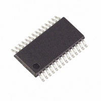
MAXQ3181-RAN+ Maxim Integrated Products, MAXQ3181-RAN+ Datasheet - Page 18

MAXQ3181-RAN+
Manufacturer Part Number
MAXQ3181-RAN+
Description
IC AFE POLYPHASE LO-PWR 28-TSSOP
Manufacturer
Maxim Integrated Products
Datasheet
1.MAXQ3181-RAN.pdf
(84 pages)
Specifications of MAXQ3181-RAN+
Number Of Channels
8
Power (watts)
35mW
Voltage - Supply, Analog
3.3V
Voltage - Supply, Digital
3.3V
Package / Case
28-TSSOP
Lead Free Status / RoHS Status
Lead free / RoHS Compliant
Number Of Bits
-
Low-Power, Active Energy, Polyphase AFE
During an SPI transfer, data is simultaneously transmit-
ted and received over two serial data lines (MISO and
MOSI) with respect to a single serial shift clock (SCLK).
The polarity and phase of the serial shift clock are the
primary components in defining the SPI data transfer
format. The polarity of the serial clock corresponds to
the idle logic state of the clock line and, therefore, also
defines which clock edge is the active edge. To define
a serial shift clock signal that idles in a logic-low state
(active clock edge = rising), the clock polarity select
(CKPOL; R_SPICF.0) bit should be configured to a 0,
while setting CKPOL = 1 causes the shift clock to idle in
a logic-high state (active clock edge = falling). The
phase of the serial clock selects which edge is used to
sample the serial shift data. The clock phase select
(CKPHA; R_SPICF.1) bit controls whether the active or
Figure 4a. SPI Interface Timing (CKPHA = 0)
Figure 4b. SPI Interface Timing (CKPHA = 1)
18
______________________________________________________________________________________
SCLK (CKPOL = 0)
SCLK (CKPOL = 1)
SCLK (CKPOL = 0)
SCLK (CKPOL = 1)
(FOR REFERENCE)
*NOT DEFINED BUT NORMALLY MSB OF CHARACTER JUST RECEIVED.
(FOR REFERENCE)
*NOT DEFINED BUT NORMALLY LSB OF PREVIOUSLY TRANSMITTED CHARACTER.
SSEL (TO SLAVE)
SSEL (TO SLAVE)
(FROM MASTER)
(FROM MASTER)
SCLK CYCLE #
(FROM SLAVE)
SCLK CYCLE #
(FROM SLAVE)
MOSI
MISO
MOSI
MISO
*
MSB
MSB
1
MSB
MSB
1
2
6
2
6
6
6
3
5
3
5
5
5
4
4
4
4
4
4
inactive clock edge is used to latch the data. When
CKPHA is set to a logic 1, data is sampled on the inac-
tive clock edge (clock returning to the idle state). When
CKPHA is set to a logic 0, data is sampled on the active
clock edge (clock transition to the active state).
Together, the CKPOL and CKPHA bits allow four possi-
ble SPI data transfer formats.
Transfers over the SPI interface always start with the
most significant bit and end with the least significant
bit. All SPI data transfers to and from the MAXQ3181
are always 8 bits (one byte) in length. The MAXQ3181
SPI interface does not support 16-bit character lengths.
The default format (upon power-up or system reset) for
the MAXQ3181 SPI interface is represented in
Figure 4a (CKPOL = 0; CKPHA = 0). In this format, the
5
3
5
3
3
3
6
2
6
2
2
2
7
1
7
1
1
1
LSB
LSB
8
LSB
8
LSB
*


