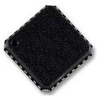
AD7195BCPZ Analog Devices Inc, AD7195BCPZ Datasheet - Page 5

AD7195BCPZ
Manufacturer Part Number
AD7195BCPZ
Description
IC AFE 24BIT 4.8K 32LFSP
Manufacturer
Analog Devices Inc
Datasheet
1.AD7195BCPZ-RL.pdf
(44 pages)
Specifications of AD7195BCPZ
Design Resources
Precision Weigh Scale Design Using AD7195 with Internal PGA and AC Excitation (CN0155)
Number Of Bits
24
Number Of Channels
4
Voltage - Supply, Analog
4.75 V ~ 5.25 V
Voltage - Supply, Digital
2.7 V ~ 5.25 V
Package / Case
32-LFCSP
Resolution (bits)
24bit
Sampling Rate
4.8kSPS
Input Channel Type
Pseudo Differential
Data Interface
3-Wire, Serial
Supply Voltage Range - Analog
4.75V To 5.25V
Lead Free Status / RoHS Status
Lead free / RoHS Compliant
Power (watts)
-
Lead Free Status / RoHS Status
Lead free / RoHS Compliant, Lead free / RoHS Compliant
Available stocks
Company
Part Number
Manufacturer
Quantity
Price
Company:
Part Number:
AD7195BCPZ
Manufacturer:
Analog Devices Inc
Quantity:
135
Company:
Part Number:
AD7195BCPZ
Manufacturer:
TST
Quantity:
5 000
Part Number:
AD7195BCPZ
Manufacturer:
ADI/亚德诺
Quantity:
20 000
Company:
Part Number:
AD7195BCPZ-RL
Manufacturer:
SEMTECH
Quantity:
394
Parameter
LOGIC INPUTS
LOGIC OUTPUT (DOUT/ RDY )
SYSTEM CALIBRATION
POWER REQUIREMENTS
1
2
3
4
5
6
7
Temperature range: −40°C to +105°C.
Specification is not production tested, but is supported by characterization data at initial product release.
FS is the decimal equivalent of Bit FS9 to Bit FS0 in the mode register.
Following a system or internal zero-scale calibration, the offset error is in the order of the noise for the programmed gain and output data rate selected. A system full-
scale calibration reduces the gain error to the order of the noise for the programmed gain and output data rate.
The analog inputs are configured for differential mode.
REJ60 is a bit in the mode register. When the output data rate is set to 50 Hz, setting REJ60 to 1 places a notch at 60 Hz, allowing simultaneous 50 Hz/60 Hz rejection.
Digital inputs equal to DV
Input High Voltage, V
Input Low Voltage, V
Hysteresis
Input Currents
Output High Voltage, V
Output Low Voltage, V
Output High Voltage, V
Output Low Voltage, V
Floating-State Leakage
Floating-State Output
Data Output Coding
Full-Scale Calibration Limit
Zero-Scale Calibration Limit
Input Span
Power Supply Voltage
AV
DV
Power Supply Currents
AI
DI
I
DD
DD
DD
Current
Capacitance
DD
DD
(Power-Down Mode)
Current
Current
− AGND
− DGND
2
2
INL
INH
7
DD
OL
OL
2
OH
OH
2
2
2
or DGND.
2
2
Min
2
0.1
−10
DV
4
−10
−1.05 × FS
0.8 × FS
4.75
2.7
DD
− 0.6
Typ
10
Offset binary
0.85
1.1
3.5
4
5
5.5
0.35
0.5
1.5
Max
0.8
0.25
+10
0.4
0.4
+10
1.05 × FS
2.1 × FS
5.25
5.25
1
1.3
4.5
5
6.4
6.9
0.4
0.6
2
Rev. 0 | Page 5 of 44
Unit
V
V
V
μA
V
V
V
V
μA
pF
V
V
V
V
V
mA
mA
mA
mA
mA
mA
mA
mA
mA
μA
Test Conditions/Comments
DV
DV
DV
DV
gain = 1, buffer off
gain = 1, buffer on
gain = 8, buffer off
gain = 8, buffer on
gain = 16 to 128, buffer off
gain = 16 to 128, buffer on
DV
DV
External crystal used
DD
DD
DD
DD
DD
DD
= 3 V, I
= 3 V, I
= 5 V, I
= 5 V, I
= 3 V
= 5 V
SOURCE
SINK
SOURCE
SINK
= 100 μA
= 1.6 mA
= 100 μA
= 200 μA
1
AD7195


