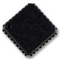
AD7195BCPZ Analog Devices Inc, AD7195BCPZ Datasheet - Page 20

AD7195BCPZ
Manufacturer Part Number
AD7195BCPZ
Description
IC AFE 24BIT 4.8K 32LFSP
Manufacturer
Analog Devices Inc
Datasheet
1.AD7195BCPZ-RL.pdf
(44 pages)
Specifications of AD7195BCPZ
Design Resources
Precision Weigh Scale Design Using AD7195 with Internal PGA and AC Excitation (CN0155)
Number Of Bits
24
Number Of Channels
4
Voltage - Supply, Analog
4.75 V ~ 5.25 V
Voltage - Supply, Digital
2.7 V ~ 5.25 V
Package / Case
32-LFCSP
Resolution (bits)
24bit
Sampling Rate
4.8kSPS
Input Channel Type
Pseudo Differential
Data Interface
3-Wire, Serial
Supply Voltage Range - Analog
4.75V To 5.25V
Lead Free Status / RoHS Status
Lead free / RoHS Compliant
Power (watts)
-
Lead Free Status / RoHS Status
Lead free / RoHS Compliant, Lead free / RoHS Compliant
Available stocks
Company
Part Number
Manufacturer
Quantity
Price
Company:
Part Number:
AD7195BCPZ
Manufacturer:
Analog Devices Inc
Quantity:
135
Company:
Part Number:
AD7195BCPZ
Manufacturer:
TST
Quantity:
5 000
Part Number:
AD7195BCPZ
Manufacturer:
ADI/亚德诺
Quantity:
20 000
Company:
Part Number:
AD7195BCPZ-RL
Manufacturer:
SEMTECH
Quantity:
394
AD7195
Table 22. Mode Register Bit Designations
Bit Location
MR23 to MR21
MR20
MR19, MR18
MR17, MR16
MR15
MR14
MR13
MR12
MR11
MR10
MR9 to MR0
Bit Name
MD2 to MD0
DAT_STA
CLK1, CLK0
0
SINC3
0
ENPAR
0
SINGLE
REJ60
FS9 to FS0
Description
Mode select bits. These bits select the operating mode of the AD7195 (see Table 23).
This bit enables the transmission of status register contents after each data register read. When
DAT_STA is set, the contents of the status register are transmitted along with each data register read.
This function is useful when several channels are selected because the status register identifies the
channel to which the data register value corresponds.
These bits select the clock source for the AD7195. Either the on-chip 4.92 MHz clock or an external
clock can be used. The ability to use an external clock allows several AD7195 devices to be synchro-
nized. Also, 50 Hz/60 Hz rejection is improved when an accurate external clock drives the AD7195.
CLK1
0
0
1
1
These bits must be programmed with a Logic 0 for correct operation.
Sinc
the sinc
For a given output data rate, f
settling time of 4/f
50 Hz/60 Hz rejection. At low output data rates, both filters give similar rms noise and similar no
missing codes for a given output data rate. At higher output data rates (FS values less than 5), the
sinc
This bit must be programmed with a Logic 0 for correct operation.
Enable parity bit. When ENPAR is set, parity checking on the data register is enabled. The DAT_STA bit
in the mode register should be set when the parity check is used. When the DAT_STA bit is set, the
contents of the status register are transmitted along with the data for each data register read.
This bit must be programmed with a Logic 0 for correct operation.
Single cycle conversion enable bit. When this bit is set, the AD7195 settles in one conversion cycle so
that it functions as a zero-latency ADC. This bit has no effect when multiple analog input channels are
enabled or when the single conversion mode is selected.
This bit enables a notch at 60 Hz when the first notch of the sinc filter is at 50 Hz. When REJ60 is set, a
filter notch is placed at 60 Hz when the sinc filter first notch is at 50 Hz. This allows simultaneous 50 Hz/
60 Hz rejection.
Filter output data rate select bits. The 10 bits of data programmed into these bits determine the filter
cut-off frequency, the position of the first notch of the filter, and the output data rate for the part. In
association with the gain selection, they also determine the output noise (and, therefore, the effective
resolution) of the device (see Table 6 through Table 17). When chop is disabled and continuous
conversion mode is selected,
where FS is the decimal equivalent of the code in Bit FS0 to Bit FS9 and is in the range 1 to 1023, and
MCLK is the master clock frequency. With a nominal MCLK of 4.92 MHz, this results in an output data
rate from 4.69 Hz to 4.8 kHz. With chop disabled, the first notch frequency is equal to the output data
rate when converting on a single channel. When chop is enabled,
where FS is the decimal equivalent of the code in Bit FS0 to Bit FS9 and is in the range 1 to 1023, and
MCLK is the master clock frequency. With a nominal MCLK of 4.92 MHz, this results in a conversion rate
from 4.69/N Hz to 4.8/N kHz, where N is the order of the sinc filter. The sinc filter’s first notch frequency
is equal to N × output data rate. The chopping introduces notches at odd integer multiples of (output
data rate/2).
Output Data Rate = (MCLK/1024)/FS
Output Data Rate = (MCLK/1024)/(N × FS)
4
3
filter gives better performance than the sinc
filter select bit. When this bit is cleared, the sinc
3
filter is used. The benefit of the sinc
CLK0
0
1
0
1
ADC
ADC Clock Source
External crystal. The external crystal is connected from MCLK1 to MCLK2.
External clock. The external clock is applied to the MCLK2 pin.
Internal 4.92 MHz clock. Pin MCLK2 is tristated.
Internal 4.92 MHz clock. The internal clock is available on MCLK2.
when chop is disabled. The sinc
Rev. 0 | Page 20 of 44
ADC
, the sinc
3
filter has a settling time of 3/f
3
filter compared to the sinc
3
filter for rms noise and no missing codes.
4
4
filter is used (default value). When this bit is set,
filter, due to its deeper notches, gives better
4
ADC
filter is its lower settling time.
while the sinc
4
filter has a


