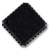
AD7195BCPZ Analog Devices Inc, AD7195BCPZ Datasheet - Page 23

AD7195BCPZ
Manufacturer Part Number
AD7195BCPZ
Description
IC AFE 24BIT 4.8K 32LFSP
Manufacturer
Analog Devices Inc
Datasheet
1.AD7195BCPZ-RL.pdf
(44 pages)
Specifications of AD7195BCPZ
Design Resources
Precision Weigh Scale Design Using AD7195 with Internal PGA and AC Excitation (CN0155)
Number Of Bits
24
Number Of Channels
4
Voltage - Supply, Analog
4.75 V ~ 5.25 V
Voltage - Supply, Digital
2.7 V ~ 5.25 V
Package / Case
32-LFCSP
Resolution (bits)
24bit
Sampling Rate
4.8kSPS
Input Channel Type
Pseudo Differential
Data Interface
3-Wire, Serial
Supply Voltage Range - Analog
4.75V To 5.25V
Lead Free Status / RoHS Status
Lead free / RoHS Compliant
Power (watts)
-
Lead Free Status / RoHS Status
Lead free / RoHS Compliant, Lead free / RoHS Compliant
Available stocks
Company
Part Number
Manufacturer
Quantity
Price
Company:
Part Number:
AD7195BCPZ
Manufacturer:
Analog Devices Inc
Quantity:
135
Company:
Part Number:
AD7195BCPZ
Manufacturer:
TST
Quantity:
5 000
Part Number:
AD7195BCPZ
Manufacturer:
ADI/亚德诺
Quantity:
20 000
Company:
Part Number:
AD7195BCPZ-RL
Manufacturer:
SEMTECH
Quantity:
394
Table 25. Channel Selection
CH7
1
DATA REGISTER
(RS2, RS1, RS0 = 0, 1, 1; Power-On/Reset = 0x000000)
The conversion result from the ADC is stored in this data register. This is a read-only, 24-bit register. On completion of a read operation
from this register, the RDY pin/bit is set. When the DAT_STA bit in the mode register is set to 1, the contents of the status register are
appended to each 24-bit conversion. This is advisable when several analog input channels are enabled because the three LSBs of the status
register (CHD2 to CHD0) identify the channel from which the conversion originated.
ID REGISTER
(RS2, RS1, RS0 = 1, 0, 0; Power-On/Reset = 0xA6)
The identification number for the AD7195 is stored in the ID register. This is a read-only register.
GPOCON REGISTER
(RS2, RS1, RS0 = 1, 0, 1; Power-On/Reset = 0x00)
The GPOCON register is an 8-bit register from which data can be read or to which data can be written. This register is used to enable the
general-purpose digital outputs.
Table 26 outlines the bit designations for the GPOCON register. GP0 through GP7 indicate the bit locations. GP denotes that the bits are
in the GPOCON register. GP7 denotes the first bit of the data stream. The number in parentheses indicates the power-on/reset default
status of that bit.
GP7
0
Table 26. Register Bit Designations
Bit Location
GP7
GP 6
GP5 to GP0
Channel Enable Bits in the Configuration Register
CH6
1
GP6
BPDSW(0)
CH5
1
0
Bit Name
BPDSW
0
CH4
1
GP5
0
CH3
1
Description
This bit must be programmed with a Logic 0 for correct operation.
Bridge power-down switch control bit. This bit is s
BPDSW to AGND. The switch can sink up to 30 mA. The bit is cleared by the user to open the bridge power-
down switch. When the ADC is placed in power-down mode, the bridge power-down switch remains active.
These bits must be programmed with a Logic 0 for correct operation.
CH2
1
CH1
1
GP4
0
CH0
1
Rev. 0 | Page 23 of 44
Positive Input
AIN(+)
AIN1
AIN3
AIN2
AIN1
AIN2
AIN3
AIN4
GP3
0
Temperature sensor
Channel Enabled
et
AIN2
AIN4
AIN2
AINCOM
AINCOM
AINCOM
AINCOM
Negative Input
AIN(−)
by the user to close the bridge power-down switch
GP2
0
Status Register
Bits CHD[2:0]
000
001
010
011
100
101
110
111
GP1
0
GP0
0
Calibration
Register Pair
0
1
None
0
0
1
2
3
AD7195


