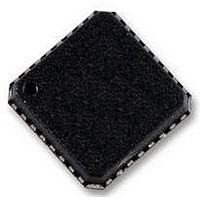
AD7195BCPZ Analog Devices Inc, AD7195BCPZ Datasheet - Page 31

AD7195BCPZ
Manufacturer Part Number
AD7195BCPZ
Description
IC AFE 24BIT 4.8K 32LFSP
Manufacturer
Analog Devices Inc
Datasheet
1.AD7195BCPZ-RL.pdf
(44 pages)
Specifications of AD7195BCPZ
Design Resources
Precision Weigh Scale Design Using AD7195 with Internal PGA and AC Excitation (CN0155)
Number Of Bits
24
Number Of Channels
4
Voltage - Supply, Analog
4.75 V ~ 5.25 V
Voltage - Supply, Digital
2.7 V ~ 5.25 V
Package / Case
32-LFCSP
Resolution (bits)
24bit
Sampling Rate
4.8kSPS
Input Channel Type
Pseudo Differential
Data Interface
3-Wire, Serial
Supply Voltage Range - Analog
4.75V To 5.25V
Lead Free Status / RoHS Status
Lead free / RoHS Compliant
Power (watts)
-
Lead Free Status / RoHS Status
Lead free / RoHS Compliant, Lead free / RoHS Compliant
Available stocks
Company
Part Number
Manufacturer
Quantity
Price
Company:
Part Number:
AD7195BCPZ
Manufacturer:
Analog Devices Inc
Quantity:
135
Company:
Part Number:
AD7195BCPZ
Manufacturer:
TST
Quantity:
5 000
Part Number:
AD7195BCPZ
Manufacturer:
ADI/亚德诺
Quantity:
20 000
Company:
Part Number:
AD7195BCPZ-RL
Manufacturer:
SEMTECH
Quantity:
394
Continuous Read
Rather than write to the communications register each time
a conversion is complete to access the data, the AD7195 can
be configured so that the conversions are placed on the
DOUT/ RDY line automatically. By writing 01011100 to
the communications register, the user need only apply the
appropriate number of SCLK cycles to the ADC, and the
conversion word is automatically placed on the DOUT/ RDY
line when a conversion is complete. The ADC should be
configured for continuous conversion mode.
When DOUT/ RDY goes low to indicate the end of a conversion,
sufficient SCLK cycles must be applied to the ADC; the data
conversion is then placed on the DOUT/ RDY line. When the
conversion is read, DOUT/ RDY returns high until the next
conversion is available. In this mode, the data can be read only
once. Also, the user must ensure that the data-word is read
before the next conversion is complete. If the user has not read
the conversion before the completion of the next conversion,
or if insufficient serial clocks are applied to the AD7195 to
read the word, the serial output register is reset when the next
DOUT/RDY
SCLK
DIN
CS
0x5C
Figure 23. Continuous Read
Rev. 0 | Page 31 of 44
DATA
conversion is complete, and the new conversion is placed in
the output serial register.
To exit the continuous read mode, Instruction 01011000 must
be written to the communications register while the RDY pin
is low. While in continuous read mode, the ADC monitors
activity on the DIN line so that it can receive the instruction
to exit the continuous read mode. Additionally, a reset occurs
if 40 consecutive 1s are seen on DIN. Therefore, DIN should
be held low in continuous read mode until an instruction is to
be written to the device.
When several channels are enabled, the ADC continuously
steps through the enabled channels and performs one con-
version on each channel each time that it is selected. DOUT/
RDY pulses low when a conversion is available. When the user
applies sufficient SCLK pulses, the data is automatically placed
on the DOUT/ RDY pin. If the DAT_STA bit in the mode
register is set to 1, the contents of the status register are output
along with the conversion. The status register indicates the
channel to which the conversion corresponds.
DATA
DATA
AD7195


