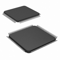
LM9833CCVJD/NOPB National Semiconductor, LM9833CCVJD/NOPB Datasheet - Page 6

LM9833CCVJD/NOPB
Manufacturer Part Number
LM9833CCVJD/NOPB
Description
IC USB IMAGE SCAN 48BIT 100-TOFP
Manufacturer
National Semiconductor
Datasheet
1.LM9833CCVJDNOPB.pdf
(42 pages)
Specifications of LM9833CCVJD/NOPB
Number Of Bits
16
Number Of Channels
3
Voltage - Supply, Analog
5V
Voltage - Supply, Digital
4.5 V ~ 5.5 V
Package / Case
100-TQFP, 100-VQFP
Lead Free Status / RoHS Status
Lead free / RoHS Compliant
Power (watts)
-
Other names
*LM9833CCVJD
*LM9833CCVJD/NOPB
LM9833CCVJD
*LM9833CCVJD/NOPB
LM9833CCVJD
Electrical Characteristics
The following specifications apply for AGND=DGND=0V, V
100%, unless otherwise noted. Boldface limits apply for T
DC and Logic Electrical Characteristics
The following specifications apply for AGND=DGND=0V, V
f
CCD/CIS Source Requirements for Full Specified Accuracy and Dynamic Range (Note 12)
Analog Input Characteristics
Internal Voltage Reference Characteristics
Digital Input Characteristics for D0-D15 (DRAM Interface)
Digital Input Characteristics for PAPER SENSE 1-2, MISC I/O 1-6, SDA, BUS POWER, CRYSTAL/EXT CLOCK, 24/48, RESET,
CMODE
Digital Input Characteristics for D+, D-
V
CRYSTAL IN
V
Symbol
V
V
CCDPEAK
V
Symbol
V
BANDGAP
REGULA-
REF MID
REF LO
V
V
V
V
V
V
REF HI
TOR
C
C
C
IN(1)
IN(0)
I
IN(1)
IN(0)
I
IN(1)
IN(0)
I
IN
IN
IN
IN
IN
IN
= 48MHz. Boldface limits apply for T
Sensor’s Maximum Output Signal
Amplitude before LM9833 Analog Front
End Saturation
Average OS
OS
Voltage Reference Output Voltage
Negative Reference Output Voltage
Midpoint Reference Output Voltage
Positive Reference Output Voltage
USB I/O Voltage Regulator
Logical “1” Input Voltage
Logical “0” Input Voltage
Input Leakage Current
Input Capacitance
Logical “1” Input Voltage
Logical “0” Input Voltage
Input Leakage Current
Input Capacitance
Logical “1” Input Voltage
Logical “0” Input Voltage
Input Leakage Current
Input Capacitance
R
, OS
G
, OS
R
, OS
Parameter
B
Parameter
Input Current
G
, OS
B
Input Current
(Continued)
A
=T
J
=T
MIN
Gain = 0.933
Gain = 3.0
Gain = 9.0
CDS Enabled, OS = 3.5V
CDS Disabled, OS = 3.5V
V
V
V
V
V
V
V
V
A
A
DRAM
DRAM
DRAM
DRAM
D
D
D
D
A
=V
=V
to T
=T
=5.25V
=4.75V
=5.25V
=4.75V
D
D
J
=V
=V
=T
MAX
=5.25V
=3.6V
=4.75V
=2.85V
6
DRAM
MIN
DRAM
; all other limits T
Conditions
Conditions
to T
=+5.0V
=+5.0V
MAX
; all other limits T
DC
DC
, f
unless otherwise noted,
DC
DC
CRYSTAL IN
A
=T
J
=25°C. (Notes 8, 9, & 10)
V
V
= 48MHz, Analog Bias Current =
REF MID
A
REF MID
(Note 9)
Typical
=T
(Note 9)
V
Typical
0.19
1.23
±26
A
1.9
0.6
3.3
±0.1
±0.1
±0.1
±3
J
/2.0
=25°C. (Notes 8, 9, & 10)
5
5
5
+1.0
-1.0
(Note 10)
(Note 10)
Limits
Limits
±30
2.0
2.0
0.8
0.8
2.0
0.8
2.0
0.8
www.national.com
µA (max)
(Limits)
(Limits)
V (max)
V (max)
V (max)
V (max)
V (min)
V (min)
V (min)
V (min)
Units
Units
nA
µA
µA
µA
pF
pF
pF
V
V
V
V
V
V
V
V


