LM9833CCVJD/NOPB National Semiconductor, LM9833CCVJD/NOPB Datasheet - Page 27

LM9833CCVJD/NOPB
Manufacturer Part Number
LM9833CCVJD/NOPB
Description
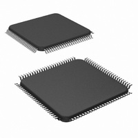
IC USB IMAGE SCAN 48BIT 100-TOFP
Manufacturer
National Semiconductor
Datasheet
1.LM9833CCVJDNOPB.pdf
(42 pages)
Specifications of LM9833CCVJD/NOPB
Number Of Bits
16
Number Of Channels
3
Voltage - Supply, Analog
5V
Voltage - Supply, Digital
4.5 V ~ 5.5 V
Package / Case
100-TQFP, 100-VQFP
Lead Free Status / RoHS Status
Lead free / RoHS Compliant
Power (watts)
-
Other names
*LM9833CCVJD
*LM9833CCVJD/NOPB
LM9833CCVJD
*LM9833CCVJD/NOPB
LM9833CCVJD
Applications Information
reaches the value stored in that color’s LAMP On register (Con-
figuration Registers 2C-37). If the On value is greater than the
value in the Line End register, then that lamp never turns on. That
color’s LAMP output goes low when the pixel counter reaches
that color’s Off value. If the Off value is greater than the value in
the Line End register, then the pixel counter will never reach the
Off value and the lamp will always stay on. Illumination Mode 2
timing is shown in Figure 21, and in slightly more detail in Figure
33.
Illumination Mode 3 is similar to Illumination Mode 2, except that
the LAMP outputs for all three colors are turned on and off every
line. Illumination Mode 3 timing is shown in Figures 22 and 23.
The Lamp On and Lamp Off settings work the same as in Mode 2
to control the on and off points for the different lamp signals. In
systems with a limited power budget, care should be taken to pre-
vent turning multiple lamps on at the same time. This can also be
important for CIS sensors that limit the maximum combined cur-
rent of the three lamps.
These modes are in operation whenever the chip is powered on
and not in standby mode. For example, the LAMP outputs in Fig-
ures 21 and 22 keep pulsing whether the LM9833 is in the Idle,
High Speed Forward or Reverse, or Scanning states. This elimi-
nates light amplitude variations due to the lamp/LEDs warm-up
characteristics. Since the LAMP pulses are synchronized to the
TR pulse, which is determined by the horizontal pixel counter, this
LAMP
LAMP
LAMP
LAMP
LAMP
LAMP
LAMP
LAMP
LAMP
TR
TR
TR
R
G
R
G
G
B
B
R
B
(LAMP
(LAMP
Figure 23: Illumination Mode 3 (green only)
Figure 22: Illumination Mode 3 (grayscale)
Figure 21: Illumination Mode 2
B
R
On > Line End, LAMP
On > Line End, LAMP
B
R
Off < Line End
Off < Line End
(Continued)
27
means that the pixel counter is constantly running, and any new
scans can only be started by waiting for the next new line (the
next Red line in the case of Illumination Mode 2).
5.2 CCD/CIS Control Block
This function generates the clock signals necessary to control a
CCD or CIS sensor. Refer to the descriptions for registers 0B to
18 for more details on the timing of specific signals. The LM9833
features:
• Independent control over the polarity (inverting or noninverting)
• Full timing control of the CIS and CDS sample points. Refer-
• Ability to turn off CDS. When CDS is on, traditional CDS is per-
• The CP1 output supplies the CP pulse needed on some popu-
• A CP2 output is another independent pixel rate pulse that (if
• CCD clock signals RS, CP1, CP2 are reset when Line Ends
• The internal Clamp signal is reset with Optical Black Pixels
• TR1 and TR2 pulse widths are always the same width, as
• The TR-Ø1 guardband may be equal to 0, causing TR and Ø1
• CIS TR1 Timing Mode 1. In this mode the TR1 pulse is exactly
• CIS TR1 Timing Mode 2. In this mode the TR pulse is again
of the input stage to accommodate CIS or CDS signals.
ence and signal sample points can be independently adjusted.
Note that the absolute time between reference sample and sig-
nal sample must be 2 MCLKs or greater, whether CDS is on or
off.
formed. When CDS is off, the signal is sampled at the Sample
Signal point, but the internal reference is used for the Sample
Reference voltage (not a point on the input signal itself).
lar Toshiba CCDs. This looks and acts just like another, inde-
pendent RS pulse.
needed) can be programmed to supply an additional clock.
End.
determined by Register 0E.
to go high simultaneously and low simultaneously (Figure 24).
This is a requirement of some Canon CIS sensors.
one Ø clock long, occurring on the rising edge of Ø1. The TR1
pulse width and guardband settings are ignored. For Dyna CIS.
equal to 1 Ø period, but now it is centered around Ø1. The TR
pulse width and guardband settings are ignored. For Canon
CIS.
TR
ø1
TR Pulse same as first clock pulse
Figure 24: TR-Ø1Guardband Can Be Equal To 0
TR1
RS
Ø1
Previous
Line
Figure 25: CIS TR1 Timing Mode 1
Transfer
Phase
Dummy
Pixels
www.national.com


