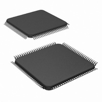
LM9833CCVJD/NOPB National Semiconductor, LM9833CCVJD/NOPB Datasheet - Page 29

LM9833CCVJD/NOPB
Manufacturer Part Number
LM9833CCVJD/NOPB
Description
IC USB IMAGE SCAN 48BIT 100-TOFP
Manufacturer
National Semiconductor
Datasheet
1.LM9833CCVJDNOPB.pdf
(42 pages)
Specifications of LM9833CCVJD/NOPB
Number Of Bits
16
Number Of Channels
3
Voltage - Supply, Analog
5V
Voltage - Supply, Digital
4.5 V ~ 5.5 V
Package / Case
100-TQFP, 100-VQFP
Lead Free Status / RoHS Status
Lead free / RoHS Compliant
Power (watts)
-
Other names
*LM9833CCVJD
*LM9833CCVJD/NOPB
LM9833CCVJD
*LM9833CCVJD/NOPB
LM9833CCVJD
Applications Information
R LED
G LED
B LED
COEF.
DATA
• 1 Channel Color: This mode uses a sensor tied to the Blue OS
R LED
G LED
B LED
COEF.
DATA
5.4 External DRAM Interface
The LM9833 supports two external DRAM sizes: 256k x 16 and
1M x 16. The DRAM is used for line buffering, gain (shading)
coefficient data, offset coefficient data, and gamma correction.
48kwords (16k pixels * 3 colors) are used for gain coefficients,
and another 48kwords (16k pixels * 3 colors) for the offset coeffi-
cients. Gamma correction consumes 12kwords (4k x 3 colors).
The remaining RAM (148kwords = 296kB for 256k DRAM, or
916kwords = 1,832kB for 1M DRAM) is used for the circular
image data buffer. The 1M size does not necessarily provide a
performance advantage (except perhaps when the USB bus is
heavily loaded and I/O is very slow) - the option is there to pro-
vide an alternative to the 256k in case of a supply shortage of
256k DRAMs.
Because the LM9833 does not use any EDO or Fast Page Mode
features, it can work with either EDO or Fast Page Mode DRAM.
The LM9833 should work with most 50-60ns 256k x 16 or 1Mx16
DRAM. Examples:
Samsung: KM416C1000C/C-L-5, KM416C1200C/C-L-5,
KM416C1004C/C-L-5, KM416C1204C/C-L-5 (5V)
KM416V1000C/C-L-5, KM416V1200C/C-L-5, KM416V1004C/C-
L-5, KM416V1204C/C-L-5 (3V)
TR
TR
input only. Illumination is switched in RGBRGB pattern at the
line rate. Each color has own digital offset and gain coefficients
as well as static Gain and Offset data. Note that there is a one
line delay between when a line is exposed to a color and when
pixels of that color are clocked out of the sensor. For example,
the Green LEDs should be on while you are clocking out Red
pixels. This mode uses Illumination Mode 2.
SC
SC = selected channel (=green in this example)
B
Figure 32: 1 Channel Grayscale
Figure 33: 1 Channel Color
SC
R
SC
G
(Continued)
SC
B
29
Alliance: AS4C1M16E5-50 (5V), AS4LC1M16E5-50 (3V)
Micron: MT4LC1M16E5DJ-5, MT4LC1M16E5TG-5 (3V)
There are 2 scan modes: 8 bit and 16 bit. The 8 bit mode is used
for normal scanning to application software to generate 8 bit gray
or 24 bit color images. The 16 bit mode is used for calibration.
The ADC always converts at 1/8 of the MCLK frequency (f
f
the HDPI divider setting (f
set correction data and the gain correction coefficient data are
provided at the DRAM datarate.
The DRAM timing is shown in Figure 34. All the read and write
operations shown in Figure 34 must be done for every pixel writ-
ten to DRAM. That limits the pixel datarate to the DRAM to
1/875ns = 1.14MHz. The following equation must be adhered to
in order to limit the DRAM datarate to 1MHz or slower:
(MCLK div)(HDPI divider)(Int Time Adj) >= 6
Int Time Adj refers to the value in register 19, and will be dis-
cussed in a later section. If register 19 = 0, then the value of Int
Time Adj = 1 (for the purpose of this equation).
5.5 PAPER SENSE and MISC I/O
These 8 pins are used for home and paper sensing, LED dis-
plays, user start buttons, etc.
Two pins are dedicated inputs: PAPER SENSE 1 and PAPER
SENSE 2. The other six pins, MISC I/O 1-6, can be configured as
48MHz
MCLK
16 bit
8 bit
7
/8). The datarate to the DRAM is the ADC rate divided by
16kwords
16kwords
16kwords
16kwords
16kwords
16kwords
4kwords
4kwords
4kwords
kwords
kwords
RO: Offset Coefficient read
RS: Shading (Gain) Coefficient read
RG: Gamma Table read
WP8: 8 bit pixel write (write 2 pixels as 16 bits
every other cycle)
WP16: 16 bit pixel write
RP: read pixel
RF: refresh
Figure 35: Memory Map of External DRAM
148
768
8 bit Datamode
1
RO
RO
Figure 34: DRAM Timing per Pixel
Red Offset
Green Offset
Blue Offset
Red Shading
Green Shading
Blue Shading
Red Gamma
Green Gamma
Blue Gamma
Pixel Data (1M)
(256k and 1M)
Pixel Data
RS
RS
2
DRAM
RG
RP
3
875ns
= f
16kwords
16kwords
16kwords
16kwords
16kwords
16kwords
ADC
kwords
kwords
WP16
WP8
160
768
/HDPI_DIVIDER. The off-
16 bit Datamode
4
Red Offset
Green Offset
Blue Offset
Red Shading
Green Shading
Blue Shading
Pixel Data (1M)
(256k and 1M)
www.national.com
Pixel Data
RP
RP
5
RF
RF
6
ADC
=


