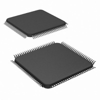
LM9833CCVJD/NOPB National Semiconductor, LM9833CCVJD/NOPB Datasheet - Page 34

LM9833CCVJD/NOPB
Manufacturer Part Number
LM9833CCVJD/NOPB
Description
IC USB IMAGE SCAN 48BIT 100-TOFP
Manufacturer
National Semiconductor
Datasheet
1.LM9833CCVJDNOPB.pdf
(42 pages)
Specifications of LM9833CCVJD/NOPB
Number Of Bits
16
Number Of Channels
3
Voltage - Supply, Analog
5V
Voltage - Supply, Digital
4.5 V ~ 5.5 V
Package / Case
100-TQFP, 100-VQFP
Lead Free Status / RoHS Status
Lead free / RoHS Compliant
Power (watts)
-
Other names
*LM9833CCVJD
*LM9833CCVJD/NOPB
LM9833CCVJD
*LM9833CCVJD/NOPB
LM9833CCVJD
Applications Information
• MISC I/O 4-6 are configured as outputs.
10.2 Soft Reset
A Soft Reset is generated by setting bit 5 of register 07. A Soft
Reset:
• Stops most of the internal clocks inside the system to save
• Does NOT stop 48MHz oscillator.
• Resets internal state machines for correct operation after
• Stops DRAM refresh. This will corrupt all the gamma, offset,
• Does NOT prevent configuration register read/writes.
The following procedure should be followed to produce a Soft
Reset:
• Set register 0x07 to 0x00 (Idle)
• Set register 0x18 to 0x18 (disabling sampling)
• Set register 0x07 to 0x20 (Reset)
• Write original value back into register 0x18, write additional
• Set register 0x07 to 0x00 (Idle)
10.3 Standby
The LM9833 enters the Standby mode by setting bit 4 of register
07. Standby Mode:
• Powers down the analog section to conserve power.
• Tristates the stepper motor outputs (regardless of the state of
• Does NOT prevent configuration register read/writes.
10.4 Suspend Mode: Entering
Suspend Mode is entered when the USB bus has had no activity
for 3ms. The Suspend state forces the LM9833 into a low current
idle state. Suspend Mode:
• Stops the oscillator.
• Forces all black-box highlighted configuration registers to their
• MISC I/O 1-3 will be configured as inputs and can be used as
10.5 Suspend Mode: Exiting
When the LM9833 exits Suspend Mode:
• The oscillator is restarted.
• The Reset and Standby bits are still set. The driver software is
11.0 USEFUL EQUATIONS
The integration time (t
where pixel_period is the time it takes to clock one pixel out of the
remote wakeup signals (after the device is initialized).
power.
register changes.
gain values, as well as any image data, stored in the external
DRAM.
configuration registers (if desired)
register 45, bit4).
default settings (including the Reset and Standby bits). See
the Reset and Standby mode descriptions for more
information.
remote wakeup signals.
responsible for clearing them and setting the configuration
registers again to resume operation. All configuration registers
and DRAM data should be re-written after a Suspend
sequence.
t INT
INT
=
) for 1 line is always:
pixel_period line_length
⋅
(Continued)
34
sensor (C = 3 for Pixel Rate Color, and 1 for all other modes):
and line_length is the length of an entire line, measured in units of
pixels. Note that this includes the transfer portion of the line:
These equations apply for any ITA (Integration Time Adjust, Reg-
ister 19) setting.
To maximize scanner throughput, it is desirable to generate data
at the same rate as the digital I/O to the host PC. Under some
conditions (slow digital I/O, or very high resolution scans), the
time to generate one line may be greater than the maximum inte-
gration time. In this case, the integration time may be set to an
acceptable value using the previous equations, and the time to
process a line extended using Register 19 (the ITA function).
Using the ITA function, the time to process 1 line can be extended
to match the digital I/O rate required:
The maximum DRAM write pixel rate allowed is 1MHz. If you con-
figure the LM9833 to generate data any faster then 1Mpixel/s, the
LM9833 will not function correctly. To ensure that the LM9833 is
programmed to a legal datarate, ensure that this constraint is
met:
When using the ITA function (ITA > 0), use this version of the
equation:
Use this equation to calculate the stepsize for a scan:
where vertical_resolution = the desired vertical resolution of the
scan, and FSPI = the number of full steps required to move the
sensor one inch.
When using the ITA function (ITA > 0), use this version of the
equation to compensate for the ITA function:
12.0 CHANGES FROM THE LM9831
12.1 FullStep Timeout Function
The LM9833 features a motor step counter that will automatically
stop the scan after a certain number of motor steps. To enable
this mode, set register 58, bit 5 = 0, then program the number of
fullsteps to scan.
12.2 16 Bit Output Mode
The LM9833’s 16 bit output mode is fully functional. It is capable
of scanning any image that the LM9833 can scan at 8 bits, and
does not require any polling of register 01.
scan_stepsize
scan_stepsize
mclk_divider HDPI_divider ITA
line_length
mclk_divider HDPI_divider
pixel_period
t
=
LINE
=
line_length vert_res
------------------------------------------------------- -
line_length vertical_resolution
---------------------------------------------------------------------------------- -
=
⋅
=
line_end
⋅
=
FSPI 4
(
1+ ITA
mclk_div C 8
--------------------------------------- -
⋅
FSPI 4
⋅
⋅
48MHz
)t
+
INT
TR_time
⋅
⋅
⋅
≥
⋅
⋅
www.national.com
6
≥
(
----------------------- -
ITA
6
ITA
+
1
)


