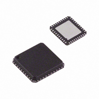
AD9571ACPZLVD Analog Devices Inc, AD9571ACPZLVD Datasheet - Page 16

AD9571ACPZLVD
Manufacturer Part Number
AD9571ACPZLVD
Description
IC PLL CLOCK GEN 25MHZ 40LFCSP
Manufacturer
Analog Devices Inc
Type
Clock Generator, Fanout Distribution, Multiplexerr
Datasheet
1.AD9571ACPZLVD.pdf
(20 pages)
Specifications of AD9571ACPZLVD
Pll
Yes
Input
Crystal
Output
CMOS, LVDS, LVPECL
Number Of Circuits
1
Ratio - Input:output
1:10
Differential - Input:output
No/Yes
Frequency - Max
156.25MHz
Divider/multiplier
Yes/No
Voltage - Supply
2.97 V ~ 3.63 V
Operating Temperature
-40°C ~ 85°C
Mounting Type
Surface Mount
Package / Case
40-LFCSP
Frequency-max
156.25MHz
Clock Ic Type
Clock Generator
Frequency
25MHz
No. Of Outputs
10
No. Of Multipliers / Dividers
1
Supply Voltage Range
3V To 3.6V
Digital Ic Case Style
LFCSP
No. Of Pins
40
Lead Free Status / RoHS Status
Lead free / RoHS Compliant
Available stocks
Company
Part Number
Manufacturer
Quantity
Price
Company:
Part Number:
AD9571ACPZLVD
Manufacturer:
AD
Quantity:
490
AD9571
The value of the resistor is dependent on the board design and
timing requirements (typically 10 Ω to 100 Ω is used). CMOS
outputs are limited in terms of the capacitive load or trace
length that they can drive. Typically, trace lengths less than
6 inches are recommended to preserve signal rise/fall times
and signal integrity.
Termination at the far end of the PCB trace is a second option.
The CMOS outputs of the AD9571 do not supply enough current
to provide a full voltage swing with a low impedance resistive,
far-end termination, as shown in Figure 16. The far-end termin-
ation network should match the PCB trace impedance and
provide the desired switching point. The reduced signal swing
may still meet receiver input requirements in some applications.
This can be useful when driving long trace lengths on less
critical nets.
LVPECL CLOCK DISTRIBUTION
The low voltage, positive emitter-coupled logic (LVPECL)
outputs of the AD9571 provide the lowest jitter clock signals
available from the AD9571. The LVPECL outputs (because they
are open emitter) require a dc termination to bias the output
transistors. The simplified equivalent circuit in Figure 13 shows
the LVPECL output stage.
In most applications, a standard LVPECL far-end termination is
recommended, as shown in Figure 17. The resistor network is
designed to match the transmission line impedance (50 Ω) and
the desired switching threshold (1.3 V).
3.3V
LVPECL
CMOS
Figure 16. CMOS Output with Far-End Termination
Figure 15. Series Termination of CMOS Output
Figure 17. LVPECL Far-End Termination
V
CMOS
10Ω
T
(NOT COUPLED)
SINGLE-ENDED
= V
CC
50Ω
50Ω
– 1.3V
10Ω
50Ω
V
MICROSTRIP
PULLUP
127Ω
1.0 INCH
83Ω
60.4Ω
3.3V
= 3.3V
100Ω
100Ω
5pF
GND
127Ω
83Ω
5pF
3.3V
LVPECL
Rev. 0 | Page 16 of 20
LVDS CLOCK DISTRIBUTION
Low voltage differential signaling (LVDS) is a second differ-
ential output option for the AD9571. LVDS uses a current mode
output stage with a factory programmed current level. The
normal value (default) for this current is 3.5 mA, which yields a
350 mV output swing across a 100 Ω resistor. The LVDS
outputs meet or exceed all ANSI/TIA/EIA-644 specifications.
A recommended termination circuit for the LVDS outputs is
shown in Figure 19.
See the AN-586 Application Note on the Analog Devices
website at
REFERENCE INPUT
By default, the crystal oscillator is enabled and used as the
reference source, which requires the connection of an external
25 MHz crystal. The REFSEL pin is pulled high internally by
about 30 kΩ to support default operation. When REFSEL is tied
low, the crystal oscillator is powered down, and the REFCLK pin
must provide a good quality 25 MHz reference clock instead.
This single-ended input can be driven by either a dc-coupled
LVCMOS level signal or an ac-coupled sine wave or square
wave, provided that an external divider is used to bias the input
at VS/2.
Table 17. REFSEL Definition
REFSEL
0
1
POWER AND GROUNDING CONSIDERATIONS AND
POWER SUPPLY REJECTION
Many applications seek high speed and performance under
less than ideal operating conditions. In these application
circuits, the implementation and construction of the PCB is as
important as the circuit design. Proper RF techniques must be
used for device selection, placement, and routing, as well as for
power supply bypassing and grounding to ensure optimum
performance.
3.3V
LVPECL
www.analog.com
Figure 18. LVPECL with Parallel Transmission Line
200Ω
LVDS
Figure 19. LVDS Output Termination
Reference Source
REFCLK input
Internal crystal oscillator
0.1nF
0.1nF
200Ω
DIFFERENTIAL
(COUPLED)
50Ω
50Ω
for more information about LVDS.
100Ω
100Ω
LVDS
3.3V
LVPECL


