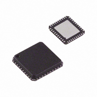
AD9571ACPZLVD Analog Devices Inc, AD9571ACPZLVD Datasheet - Page 10

AD9571ACPZLVD
Manufacturer Part Number
AD9571ACPZLVD
Description
IC PLL CLOCK GEN 25MHZ 40LFCSP
Manufacturer
Analog Devices Inc
Type
Clock Generator, Fanout Distribution, Multiplexerr
Datasheet
1.AD9571ACPZLVD.pdf
(20 pages)
Specifications of AD9571ACPZLVD
Pll
Yes
Input
Crystal
Output
CMOS, LVDS, LVPECL
Number Of Circuits
1
Ratio - Input:output
1:10
Differential - Input:output
No/Yes
Frequency - Max
156.25MHz
Divider/multiplier
Yes/No
Voltage - Supply
2.97 V ~ 3.63 V
Operating Temperature
-40°C ~ 85°C
Mounting Type
Surface Mount
Package / Case
40-LFCSP
Frequency-max
156.25MHz
Clock Ic Type
Clock Generator
Frequency
25MHz
No. Of Outputs
10
No. Of Multipliers / Dividers
1
Supply Voltage Range
3V To 3.6V
Digital Ic Case Style
LFCSP
No. Of Pins
40
Lead Free Status / RoHS Status
Lead free / RoHS Compliant
Available stocks
Company
Part Number
Manufacturer
Quantity
Price
Company:
Part Number:
AD9571ACPZLVD
Manufacturer:
AD
Quantity:
490
AD9571
PIN CONFIGURATION AND FUNCTION DESCRIPTIONS
Table 13. Pin Function Descriptions
Pin No.
2
3, 4, 29, 30, 31, 32
5
6, 7
8
9
11
1, 10, 34
14, 36
15
16
17
18
19, 21
20, 22
23
24
25
26
27
28
Mnemonic
VS
25M
VS
XO
REFCLK
REFSEL
VS
GND
BYPASS2, BYPASS1
VS
VS
156M
156M
100M/125M
100M /
33M
VS
VS
VS
FREQSEL
VS
125M
NOTES
1. * = SHORT TO PIN 36.
2. ** = SHORT TO PIN 14.
3. NOTE THAT THE EXPOSED PADDLE ON THIS PACKAGE IS AN ELECTRICAL
CONNECTION AS WELL AS A THERMAL ENHANCEMENT. FOR THE DEVICE TO
FUNCTION PROPERLY, THE PADDLE MUST BE ATTACHED TO GROUND (GND).
1
REFCLK
REFSEL
GND
GND
Description
Power Supply Connection for the 25M CMOS Buffer.
CMOS 25 MHz Output.
Power Supply Connection for the Crystal Oscillator.
External 25 MHz Crystal.
25 MHz Reference Clock Input. Tie low when not in use.
Logic Input. Used to select the reference source.
Power Supply Connection for the GbE PLL.
Ground Pins. The external paddle must be attached to GND.
These pins are for bypassing each LDO to ground with a 220 nF capacitor.
Power Supply Connection for the GbE VCO.
Power Supply Connection for the 156M LVDS Output Buffer and Output Dividers.
LVPECL/LVDS Output at 156.25 MHz.
Complementary LVPECL/LVDS Output at 156.25 MHz.
LVPECL/LVDS Output at 100 MHz or 125 MHz. Selected by FREQSEL pin strapping.
Complementary LVPECL/LVDS Output at 100 MHz or 125 MHz.
CMOS 33.33 MHz Output.
Power Supply Connection for the 33M CMOS Output Buffer and Output Dividers.
Power Supply Connection for the 100M/125M LVDS Output Buffer and Output Dividers.
Power Supply Connection for the GbE PLL Feedback Divider.
Logic Input. Used to configure output drivers.
Power Supply Connection for the FC PLL Feedback Divider.
25M
25M
XO
XO
VS
VS
10
1
2
3
4
5
6
7
8
9
Figure 6. Pin Configuration
PIN 1
INDICATOR
Rev. 0 | Page 10 of 20
(Not to Scale)
AD9571
TOP VIEW
LVPECL/
LVDS
30 25M
29 25M
28 VS
27 FREQSEL
26 VS
25 VS
24 VS
23 33M
22 100M/125M
21 100M/125M


