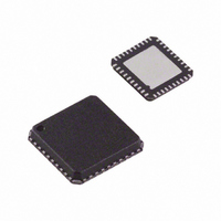
AD9571ACPZLVD Analog Devices Inc, AD9571ACPZLVD Datasheet - Page 14

AD9571ACPZLVD
Manufacturer Part Number
AD9571ACPZLVD
Description
IC PLL CLOCK GEN 25MHZ 40LFCSP
Manufacturer
Analog Devices Inc
Type
Clock Generator, Fanout Distribution, Multiplexerr
Datasheet
1.AD9571ACPZLVD.pdf
(20 pages)
Specifications of AD9571ACPZLVD
Pll
Yes
Input
Crystal
Output
CMOS, LVDS, LVPECL
Number Of Circuits
1
Ratio - Input:output
1:10
Differential - Input:output
No/Yes
Frequency - Max
156.25MHz
Divider/multiplier
Yes/No
Voltage - Supply
2.97 V ~ 3.63 V
Operating Temperature
-40°C ~ 85°C
Mounting Type
Surface Mount
Package / Case
40-LFCSP
Frequency-max
156.25MHz
Clock Ic Type
Clock Generator
Frequency
25MHz
No. Of Outputs
10
No. Of Multipliers / Dividers
1
Supply Voltage Range
3V To 3.6V
Digital Ic Case Style
LFCSP
No. Of Pins
40
Lead Free Status / RoHS Status
Lead free / RoHS Compliant
Available stocks
Company
Part Number
Manufacturer
Quantity
Price
Company:
Part Number:
AD9571ACPZLVD
Manufacturer:
AD
Quantity:
490
AD9571
THEORY OF OPERATION
Figure 11 shows a block diagram of the AD9571. The chip
consists of a PLL core, which is configured to generate the
specific clock frequencies required for Ethernet applications,
without any user programming. This PLL is based on proven
Analog Devices synthesizer technology, noted for its exceptional
phase noise performance. The AD9571 is highly integrated and
includes loop filters, regulators for supply noise immunity, all
the necessary dividers with multiple output buffers in a choice
of formats, and a crystal oscillator. A user need only supply a
25 MHz reference clock or an external crystal to implement an
entire line card clocking solution that does not require any
processor intervention. Six copies of the 25 MHz reference
source are also available.
REFCLK
XTAL
OSC
REFSEL VS
1
0
FREQUENCY
AD9571
DETECTOR
CHARGE
PHASE
PUMP
V
LDO
GND
Figure 11. Detailed Block Diagram
VCO
Rev. 0 | Page 14 of 20
DIVIDE
DIVIDE
DIVIDE
BY 25
BY 4
BY 5
OUTPUTS
Table 14 provides a summary of the outputs available.
Table 14. Output Formats
Frequency
25 MHz
156.25 MHz
100 MHz or 125 MHz
33.33 MHz
Note that the pins labeled 100M/125M can provide 100 MHz or
125 MHz by strapping the FREQSEL pin as shown in Table 15.
DIVIDE
DIVIDE
DIVIDE
DIVIDE
BY 4
BY 4
BY 5
BY 3
DECODE
LEVEL
0
1
0
1
FORCE_LOW
156.25MHz
LVPECL/
LVPECL/
LVPECL/
125MHz/
125MHz/
100MHz
100MHz
LVDS
LVDS
LVDS
33.33MHz
25MHz
CMOS
CMOS
CMOS
CMOS
Format
CMOS
LVPECL/LVDS
LVPECL/LVDS
CMOS
25M
25M
25M
25M
25M
25M
33M
156M
156M
100M/125M
100M/125M
FREQSEL
100M/125M
100M/125M
Copies
6
1
2
1


