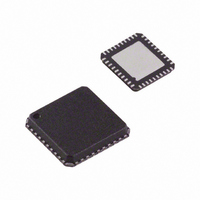
AD9571ACPZLVD Analog Devices Inc, AD9571ACPZLVD Datasheet - Page 15

AD9571ACPZLVD
Manufacturer Part Number
AD9571ACPZLVD
Description
IC PLL CLOCK GEN 25MHZ 40LFCSP
Manufacturer
Analog Devices Inc
Type
Clock Generator, Fanout Distribution, Multiplexerr
Datasheet
1.AD9571ACPZLVD.pdf
(20 pages)
Specifications of AD9571ACPZLVD
Pll
Yes
Input
Crystal
Output
CMOS, LVDS, LVPECL
Number Of Circuits
1
Ratio - Input:output
1:10
Differential - Input:output
No/Yes
Frequency - Max
156.25MHz
Divider/multiplier
Yes/No
Voltage - Supply
2.97 V ~ 3.63 V
Operating Temperature
-40°C ~ 85°C
Mounting Type
Surface Mount
Package / Case
40-LFCSP
Frequency-max
156.25MHz
Clock Ic Type
Clock Generator
Frequency
25MHz
No. Of Outputs
10
No. Of Multipliers / Dividers
1
Supply Voltage Range
3V To 3.6V
Digital Ic Case Style
LFCSP
No. Of Pins
40
Lead Free Status / RoHS Status
Lead free / RoHS Compliant
Available stocks
Company
Part Number
Manufacturer
Quantity
Price
Company:
Part Number:
AD9571ACPZLVD
Manufacturer:
AD
Quantity:
490
Table 15. FREQSEL Definition
FREQSEL
0
1
NC
The simplified equivalent circuits of the LVDS and LVPECL
outputs are shown in Figure 12 and Figure 13.
The differential outputs are factory programmed to either LVPECL
or LVDS format, and either option can be sampled on request.
CMOS drivers tend to generate more noise than differential
outputs and, as a result, the proximity of the 33.33 MHz output
to Pin 21 and Pin 22 does affect the jitter performance when
FREQSEL = 0 (that is, when the differential output is generating
125 MHz). For this reason, the 33.33 MHz pin can be forced to
a low state by asserting the FORCE_LOW signal on Pin 37 (see
Table 16). An internal pull-down enables the 33.33 MHz output
if the pin is not connected.
Table 16. FORCE_LOW (Pin 37) Definition
FORCE_LOW
0 or NC
1
Figure 13. LVPECL Output Simplified Equivalent Circuit
Figure 12. LVDS Output Simplified Equivalent Circuit
Frequency Available
from Pin 19 and Pin 20
(MHZ)
125
100
125
33.33 MHz Output (Pin 23)
33.33 MHz
0 MHz
3.5mA
3.5mA
GND
3.3V
OUT
OUT
Frequency Available
from Pin 21 and Pin 22
(MHZ)
125
100
100
OUT
OUT
Rev. 0 | Page 15 of 20
PHASE FREQUENCY DETECTOR (PFD) AND
CHARGE PUMP
The PFD takes inputs from the reference clock and feedback
divider to produce an output proportional to the phase and
frequency difference between them. Figure 14 shows a
simplified schematic.
POWER SUPPLY
The AD9571 requires a 3.3 V ± 10% power supply for V
Specifications section gives the performance expected from the
AD9571 with the power supply voltage within this range. The
absolute maximum range of (−0.3 V) − (+3.6 V), with respect to
GND, must never be exceeded on the VS pin.
Good engineering practice should be followed in the layout of
power supply traces and the ground plane of the PCB. Bypass
the power supply on the PCB with adequate capacitance (>10
µF). Bypass the AD9571 with adequate capacitors (0.1 µF) at all
power pins as close as possible to the part. The layout of the
AD9571 evaluation board is a good example.
The exposed metal paddle on the AD9571 package is an electrical
connection, as well as a thermal enhancement. For the device to
function properly, the paddle must be properly attached to ground
(GND). The PCB acts as a heat sink for the AD9571; therefore,
this GND connection should provide a good thermal path to a
larger dissipation area, such as a ground plane on the PCB.
CMOS CLOCK DISTRIBUTION
The AD9571 provides seven CMOS clock outputs (six 25 MHz
and one 33.33 MHz) that are dedicated CMOS levels. Whenever
single-ended CMOS clocking is used, some of the following
general guidelines should be followed.
Point-to-point nets should be designed such that a driver has
one receiver only on the net, if possible. This allows for simple
termination schemes and minimizes ringing due to possible
mismatched impedances on the net. Series termination at the
source is generally required to provide transmission line
matching and/or to reduce current transients at the driver.
FEEDBACK
DIVIDER
REFCLK
HIGH
HIGH
Figure 14. PFD Simplified Schematic
D1 Q1
D2 Q2
CLR1
CLR2
UP
DOWN
GND
3.3V
CHARGE
PUMP
CP
AD9571
S
. The


