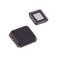
ADF4360-0BCPZ Analog Devices Inc, ADF4360-0BCPZ Datasheet - Page 19

ADF4360-0BCPZ
Manufacturer Part Number
ADF4360-0BCPZ
Description
IC INTEGRATED SYNTH/VCO 24-LFCSP
Manufacturer
Analog Devices Inc
Type
Fanout Distribution, Integer N Synthesizer (RF)r
Datasheet
1.ADF4360-0BCPZ.pdf
(24 pages)
Specifications of ADF4360-0BCPZ
Pll
Yes
Input
CMOS
Output
Clock
Number Of Circuits
1
Ratio - Input:output
1:2
Differential - Input:output
No/No
Frequency - Max
2.725GHz
Divider/multiplier
Yes/No
Voltage - Supply
3 V ~ 3.6 V
Operating Temperature
-40°C ~ 85°C
Mounting Type
Surface Mount
Package / Case
24-LFCSP
Frequency-max
2.725GHz
Pll Type
Frequency Synthesis
Frequency
2.725GHz
Supply Current
10mA
Supply Voltage Range
3V To 3.6V
Digital Ic Case Style
LFCSP
No. Of Pins
24
Operating Temperature Range
-40°C To +85°C
Lead Free Status / RoHS Status
Lead free / RoHS Compliant
For Use With
EVAL-ADF4360-0EBZ1 - BOARD EVALUATION FOR ADF4360-0
Lead Free Status / RoHS Status
Lead free / RoHS Compliant, Lead free / RoHS Compliant
N COUNTER LATCH
With (C2, C1) = (1, 0), the N counter latch is programmed.
Table 8 shows the input data format for programming the
N counter latch.
A Counter Latch
A5 to A1 program the 5-bit A counter. The divide range is 0
(00000) to 31 (11111).
Reserved Bits
DB7 is a spare bit that is reserved. It should be programmed to 0.
B Counter Latch
B13 to B1 program the B counter. The divide range is 3
(00.....0011) to 8191 (11....111).
Overall Divide Range
The overall divide range is defined by ((P × B) + A), where P is
the prescaler value.
CP Gain
DB21 of the N counter latch in the ADF4360 family is the
charge pump gain bit. When this is programmed to 1, Current
Setting 2 is used. When programmed to 0, Current Setting 1 is used.
This bit can also be programmed through DB10 of the control
latch. The bit always reflects the latest value written to it, whether
this is through the control latch or the N counter latch.
Divide-by-2
DB22 is the divide-by-2 bit. When set to 1, the output divide-by-2
function is chosen. When it is set to 0, normal operation occurs.
Divide-by-2 Select
DB23 is the divide-by-2 select bit. When programmed to 1, the
divide-by-2 output is selected as the prescaler input. When set
to 0, the fundamental is used as the prescaler input. For exam-
ple, using the output divide-by-2 feature and a PFD frequency
of 200 kHz, the user needs a value of N = 13,000 to generate
1,500 MHz. With the divide-by-2 select bit high, the user may
keep N = 6,500.
Rev. A | Page 19 of 24
R COUNTER LATCH
With (C2, C1) = (0, 1), the R counter latch is programmed.
Table 9 shows the input data format for programming the
R counter latch.
R Counter
R1 to R14 set the counter divide ratio. The divide range is 1
(00......001) to 16383 (111......111).
Antibacklash Pulse Width
DB16 and DB17 set the antibacklash pulse width.
Lock Detect Precision
DB18 is the lock detect precision bit. This bit sets the number of
reference cycles with less than 15 ns phase error for entering the
locked state. With LDP at 1, five cycles are taken; with LDP at 0,
three cycles are taken.
Test Mode Bit
DB19 is the test mode bit (TMB) and should be set to 0. With
TMB = 0, the contents of the test mode latch are ignored and
normal operation occurs as determined by the contents of the
control latch, R counter latch, and N counter latch. Note that
test modes are for factory testing only and should not be pro-
grammed by the user.
Band Select Clock
These bits set a divider for the band select logic clock input. The
output of the R counter is by default the value used to clock the
band select logic, but, if this value is too high (>1 MHz), a
divider can be switched on to divide the R counter output to a
smaller value (see Table 9).
Reserved Bits
DB23 to DB22 are spare bits that are reserved. They should be
programmed to 0.
ADF4360-0


