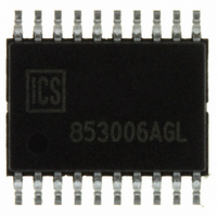
ICS853006AGLF IDT, Integrated Device Technology Inc, ICS853006AGLF Datasheet - Page 6

ICS853006AGLF
Manufacturer Part Number
ICS853006AGLF
Description
IC FANOUT BUFFER LVPECL 20-TSSOP
Manufacturer
IDT, Integrated Device Technology Inc
Series
HiPerClockS™r
Type
Fanout Buffer (Distribution)r
Specifications of ICS853006AGLF
Number Of Circuits
1
Ratio - Input:output
1:6
Differential - Input:output
Yes/Yes
Input
CML, LVDS, LVPECL, SSTL
Output
ECL, LVPECL
Frequency - Max
2GHz
Voltage - Supply
2.375 V ~ 3.465 V
Operating Temperature
-40°C ~ 85°C
Mounting Type
Surface Mount
Package / Case
20-TSSOP
Frequency-max
2GHz
Number Of Outputs
12
Operating Supply Voltage (max)
-3.465/3.465V
Operating Temp Range
-40C to 85C
Propagation Delay Time
0.51ns
Operating Supply Voltage (min)
-2.375/2.375V
Mounting
Surface Mount
Pin Count
20
Operating Supply Voltage (typ)
-2.5/-3.3/3.3V
Package Type
TSSOP
Operating Temperature Classification
Industrial
Lead Free Status / RoHS Status
Lead free / RoHS Compliant
Other names
800-1157
800-1157-5
800-1157
853006AGLF
800-1157-5
800-1157
853006AGLF
IDT™ / ICS™ LOW SKEW, 1-TO-6 DIFFERENTIAL-TO-2.5V/3.3V LVPECL/ECL FANOUT BUFFER
ICS853006
LOW SKEW, 1-TO-6 DIFFERENTIAL-TO-2.5V/3.3V LVPECL/ECL FANOUT BUFFER
853006AG
The spectral purity in a band at a specific offset from the funda-
mental compared to the power of the fundamental is called the
dBc Phase Noise. This value is normally expressed using a
Phase noise plot and is most often the specified plot in many
applications. Phase noise is defined as the ratio of the noise
power present in a 1Hz band at a specified offset from the fun-
damental frequency to the power value of the fundamental. This
ratio is expressed in decibels (dBm) or a ratio of the power in
As with most timing specifications, phase noise measurements
have issues. The primary issue relates to the limitations of the
equipment. Often the noise floor of the equipment is higher than
the noise floor of the device. This is illustrated above. The de-
-100
-110
-120
-130
-140
-150
-160
-170
-180
-190
-10
-20
-30
-40
-50
-60
-70
-80
-90
0
1k
Integrated
Circuit
Systems, Inc.
10k
D
IFFERENTIAL
www.icst.com/products/hiperclocks.html
O
A
FFSET
DDITIVE
100k
F
ROM
-
TO
P
C
HASE
6
-2.5V/3.3V LVPECL/ECL F
6
ARRIER
the 1Hz band to the power in the fundamental. When the re-
quired offset is specified, the phase noise is called a dBc value,
which simply means dBm at a specified offset from the funda-
mental. By investigating jitter in the frequency domain, we get a
better understanding of its effects on the desired application over
the entire time record of the signal. It is mathematically possible
to calculate an expected bit error rate given a phase noise plot.
vice meets the noise floor of what is shown, but can actually be
lower. The phase noise is dependant on the input source and
measurement equipment.
J
F
ITTER
REQUENCY
1M
(H
Z
)
Phase Jitter
Input/Output Additive
10M
L
OW
= 0.03ps (typical)
ANOUT
REV. A NOVEMBER 9, 2004
at 155.52MHz
S
KEW
, 1-
B
UFFER
TO
100M
ICS853006
-6
TSD


