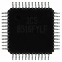
ICS8516FYLF IDT, Integrated Device Technology Inc, ICS8516FYLF Datasheet - Page 6

ICS8516FYLF
Manufacturer Part Number
ICS8516FYLF
Description
IC CLK DISTR 1:16 LVDS 48-LQFP
Manufacturer
IDT, Integrated Device Technology Inc
Series
HiPerClockS™r
Type
Fanout Buffer (Distribution)r
Datasheet
1.ICS8516FYLF.pdf
(16 pages)
Specifications of ICS8516FYLF
Number Of Circuits
1
Ratio - Input:output
1:16
Differential - Input:output
Yes/Yes
Input
HCSL, LVDS, LVHSTL, LVPECL, SSTL
Output
LVDS
Frequency - Max
700MHz
Voltage - Supply
3.135 V ~ 3.465 V
Operating Temperature
0°C ~ 70°C
Mounting Type
Surface Mount
Package / Case
48-LQFP
Frequency-max
700MHz
Number Of Outputs
32
Operating Supply Voltage (max)
3.465V
Operating Temp Range
0C to 70C
Propagation Delay Time
5ns
Operating Supply Voltage (min)
3.135V
Mounting
Surface Mount
Pin Count
48
Operating Supply Voltage (typ)
3.3V
Package Type
TQFP
Duty Cycle
55%
Operating Temperature Classification
Commercial
Lead Free Status / RoHS Status
Lead free / RoHS Compliant
Other names
800-1154
8516FYLF
8516FYLF
Available stocks
Company
Part Number
Manufacturer
Quantity
Price
Company:
Part Number:
ICS8516FYLF
Manufacturer:
AD
Quantity:
1 722
Company:
Part Number:
ICS8516FYLF
Manufacturer:
IDT, Integrated Device Technology Inc
Quantity:
10 000
Company:
Part Number:
ICS8516FYLFT
Manufacturer:
IDT, Integrated Device Technology Inc
Quantity:
10 000
IDT™ / ICS™ LOW SKEW, 1-TO-16 DIFFERENTIAL-TO-LVDS CLOCK DISTRIBUTION CHIP
ICS8516
LOW SKEW, 1-TO-16 DIFFERENTIAL-TO-LVDS CLOCK DISTRIBUTION CHIP
8516FY
The spectral purity in a band at a specific offset from the
fundamental compared to the power of the fundamental is
called the dBc Phase Noise. This value is normally expressed
using a Phase noise plot and is most often the specified plot
in many applications. Phase noise is defined as the ratio of
the noise power present in a 1Hz band at a specified offset
from the fundamental frequency to the power value of the
fundamental. This ratio is expressed in decibels (dBm) or a
As with most timing specifications, phase noise measure-
ments have issues. The primary issue relates to the limita-
tions of the equipment. Often the noise floor of the equipment
is higher than the noise floor of the device. This is illustrated
-100
-100
-120
-130
-140
-150
-160
-50
-60
-70
-80
-90
1k
Integrated
Circuit
Systems, Inc.
10k
www.icst.com/products/hiperclocks.html
A
DDITIVE
O
FFSET
100k
D
F
IFFERENTIAL
ROM
P
HASE
6
6
C
ratio of the power in the 1Hz band to the power in the funda-
mental. When the required offset is specified, the phase noise
is called a dBc value, which simply means dBm at a specified
offset from the fundamental. By investigating jitter in the fre-
quency domain, we get a better understanding of its effects
on the desired application over the entire time record of the
signal. It is mathematically possible to calculate an expected
bit error rate given a phase noise plot.
ARRIER
above. The device meets the noise floor of what is shown, but
can actually be lower. The phase noise is dependant on the
input source and measurement equipment.
J
F
ITTER
REQUENCY
Additive Phase Jitter
-
TO
1M
-LVDS C
(H
Z
)
LOCK
(12kHz to 20MHz)
= 148fs typical
L
@ 155.52MHz
OW
D
10M
ISTRIBUTION
S
KEW
REV. B FEBRUARY 21, 2006
, 1-
TO
C
-16
HIP
100M
ICS8516
TSD


