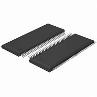
ICS9DB1200CGLF IDT, Integrated Device Technology Inc, ICS9DB1200CGLF Datasheet

ICS9DB1200CGLF
Specifications of ICS9DB1200CGLF
Available stocks
Related parts for ICS9DB1200CGLF
ICS9DB1200CGLF Summary of contents
Page 1
Twelve Output Differential Buffer for PCIe Gen1/Gen2, QPI, and FBDIMM Description DB1200 Rev 2.0 Intel Yellow Cover Device Description The ICS9DB1200 is an Intel DB1200 Differential Buffer Specification device. This buffer provides 12 differential clocks at frequencies ranging from 100MHz ...
Page 2
ICS9DB1200C Twelve Output Differential Buffer for PCIe Gen1/Gen2, QPI, and FBDIMM Pin Configuration Frequency Select Table B0b2 B0b1 B0b0 ...
Page 3
ICS9DB1200C Twelve Output Differential Buffer for PCIe Gen1/Gen2, QPI, and FBDIMM Pin Description PIN # PIN NAME 1 VDD 2 DIF_IN 3 DIF_IN# 4 GND 5 OE0# 6 DIF_0 7 DIF_0# 8 VDD 9 GND 10 OE1# 11 DIF_1 12 ...
Page 4
ICS9DB1200C Twelve Output Differential Buffer for PCIe Gen1/Gen2, QPI, and FBDIMM Pin Description PIN # PIN NAME 33 SMBDAT 34 FS1 35 BYPASS#/PLL 36 VTTPWRGD#/PD 37 DIF_6# 38 DIF_6 39 OE6# 40 GND 41 VDD 42 DIF_7# 43 DIF_7 44 ...
Page 5
ICS9DB1200C Twelve Output Differential Buffer for PCIe Gen1/Gen2, QPI, and FBDIMM Absolute Max Symbol Parameter VDDA 3.3V Core Supply Voltage VDD 3.3V Logic Supply Voltage V Input Low Voltage IL V Input High Voltage IH Ts Storage Temperature Tambient Ambient ...
Page 6
ICS9DB1200C Twelve Output Differential Buffer for PCIe Gen1/Gen2, QPI, and FBDIMM Electrical Characteristics - Clock Input Parameters 70°C; Supply Voltage V = 3.3 V +/- PARAMETER SYMBOL Input High Voltage - V IHDIF DIF_IN ...
Page 7
ICS9DB1200C Twelve Output Differential Buffer for PCIe Gen1/Gen2, QPI, and FBDIMM Electrical Characteristics - Phase Jitter PARAMETER SYMBOL Jitter, Phase tjphase Notes on Phase Jitter: 1 See http://www.pcisig.com for complete specs. Guaranteed by design and characterization, not tested in production. ...
Page 8
ICS9DB1200C Twelve Output Differential Buffer for PCIe Gen1/Gen2, QPI, and FBDIMM Common Recommendations for Differential Routing L1 length, Route as non-coupled 50 ohm trace. L2 length, Route as non-coupled 50 ohm trace. L3 length, Route as non-coupled 50 ohm trace. ...
Page 9
ICS9DB1200C Twelve Output Differential Buffer for PCIe Gen1/Gen2, QPI, and FBDIMM Alternative termination for LVDS and other common differential signals. Vdiff Vp-p Vcm 0.45 v 0.22v 1.08 0.58 0.6 0.28 0.80 0.40 0.6 0.60 1.2 0.3 R1a = R1b = ...
Page 10
ICS9DB1200C Twelve Output Differential Buffer for PCIe Gen1/Gen2, QPI, and FBDIMM General SMBus serial interface information for the ICS9DB1200C How to Write: • Controller (host) sends a start bit. • Controller (host) sends the write address DC • ICS clock ...
Page 11
ICS9DB1200C Twelve Output Differential Buffer for PCIe Gen1/Gen2, QPI, and FBDIMM SMBus Table: Frequency Select Register Byte 0 Pin # Name Bit 7 - HIGH_BW# Bit 6 - BYPASS#/PLL Bit 5 - Reserved Bit 4 - Reserved Bit 3 - ...
Page 12
ICS9DB1200C Twelve Output Differential Buffer for PCIe Gen1/Gen2, QPI, and FBDIMM SMBus Table: Output Enable Readback Byte 4 Pin # Name - Reserved Bit 7 Bit 6 - Reserved Bit 5 - Reserved Bit 4 - Reserved Bit 3 58,59 ...
Page 13
ICS9DB1200C Twelve Output Differential Buffer for PCIe Gen1/Gen2, QPI, and FBDIMM INDEX INDEX AREA AREA Ordering Information Part / Order Number Shipping Packaging 9DB1200CGLF 9DB1200CGLFT Tape and ...
Page 14
ICS9DB1200C Twelve Output Differential Buffer for PCIe Gen1/Gen2, QPI, and FBDIMM Revision History Rev. Issue Date Description 1. Updated SMBus Serial Interface Information. A 12/18/2007 2. Release to Final. B 4/7/2008 Added Input Clock Parameters 1. Updated Phase Jitter Numbers ...


