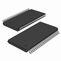
ICS9DB801CGLF IDT, Integrated Device Technology Inc, ICS9DB801CGLF Datasheet - Page 7

ICS9DB801CGLF
Manufacturer Part Number
ICS9DB801CGLF
Description
IC BUFFER 8OUTPUT DIFF 48-TSSOP
Manufacturer
IDT, Integrated Device Technology Inc
Type
Clock Bufferr
Series
-r
Datasheet
1.ICS9DB801CGLFT.pdf
(19 pages)
Specifications of ICS9DB801CGLF
Input
Clock
Output
Clock
Frequency - Max
400MHz
Voltage - Supply
3.135 V ~ 3.465 V
Operating Temperature
0°C ~ 70°C
Mounting Type
Surface Mount
Package / Case
48-TSSOP
Frequency-max
400MHz
Number Of Elements
1
Supply Current
200mA
Pll Input Freq (min)
50MHz
Pll Input Freq (max)
200MHz
Operating Supply Voltage (typ)
3.3V
Operating Temp Range
0C to 70C
Package Type
TSSOP
Output Frequency Range
50 to 200MHz
Operating Supply Voltage (min)
3.135V
Operating Supply Voltage (max)
3.465V
Operating Temperature Classification
Commercial
Pin Count
48
Lead Free Status / RoHS Status
Lead free / RoHS Compliant
Other names
9DB801CGLF
Available stocks
Company
Part Number
Manufacturer
Quantity
Price
Company:
Part Number:
ICS9DB801CGLF
Manufacturer:
IDT
Quantity:
5 390
Absolute Max
Electrical Characteristics - Input/Supply/Common Output Parameters
IDT
T
Operating Supply Current
1
2
3
Tambient
ESD prot
Guaranteed by design and characterization, not 100% tested in production.
See timing diagrams for timing requirements.
Time from deassertion until outputs are >200 mV
Symbol
VDD_In
VDD_A
A
Modulation Frequency
Tcase
ICS9DB801C
Eight Output Differential Buffer for PCI Express (50-200MHz)
Tdrive_SRC_STOP#
Powerdown Current
= 0 - 70°C; Supply Voltage V
Input Capacitance
TM
Input High Voltage
Input High Current
Clk Stabilization
Input Low Voltage
V
V
Input Low Current
Ts
Input Frequency
Input Frequency
Input Frequency
Pin Inductance
PLL Bandwidth
/ICS
IL
IH
PARAMETER
Tdrive_PD#
TM
Trise
Tfall
Eight Output Differential Buffer for PCI Express (50-200MHz)
3.3V Logic Supply Voltage
3.3V Core Supply Voltage
Ambient Operating Temp
Storage Temperature
Input ESD protection
human body model
Input Low Voltage
Input High Voltage
Case Temperature
1,2
1
1
Parameter
I
SYMBOL
DD3.3ByPass
I
I
F
F
DD3.3PLL
fMOD
DD3.3PD
T
F
C
iBypass
iBypass
BW
V
L
C
V
I
I
STAB
I
IL1
IL2
iPLL
OUT
IH
pin
DD
IH
IN
IL
= 3.3 V +/-5%
input clock stabilization or de-
V
From V
assertion of PD# to 1st clock
V
all differential pairs tri-stated
IN
Full Active, C
IN
SRC_Stop# de-assertion
Bypass Mode (Revision
Bypass Mode (Revision
Output pin capacitance
DIF output enable after
DIF output enable after
= 0 V; Inputs with no pull-
= 0 V; Inputs with pull-up
Triangular Modulation
Rise time of PD# and
PLL Bandwidth when
PLL Bandwidth when
Fall time of PD# and
all diff pairs driven
PD# de-assertion
B/REV ID = 1H)
C/REV ID = 2H)
DD
CONDITIONS
SRC_STOP#
SRC_STOP#
Logic Inputs
3.3 V +/-5%
3.3 V +/-5%
up resistors
PLL_BW=0
PLL_BW=1
GND-0.5
PLL Mode
V
Power-Up and after
resistors
2000
IN
Min
-65
0
= V
L
= Full load;
DD
V
DD
Max
150
115
4.6
4.6
+0.5V
70
GND - 0.3
7
MIN
-200
1.5
2.4
0.7
50
30
-5
-5
2
0
0
Units
°
°C
°C
V
V
V
V
V
C
TYP
175
160
0.5
50
10
1
3
1
V
333.33
DD
MAX
200
175
200
400
300
0.8
3.4
1.4
70
33
15
5
4
7
4
4
1
5
5
+ 0.3
UNITS NOTES
MHz
MHz
MHz
MHz
MHz
kHz
mA
mA
mA
mA
ms
uA
uA
uA
nH
pF
pF
ns
us
ns
ns
V
V
1,2
1,3
1,3
1
1
1
1
1
1
1
2
9DB801C
REV E 01/27/11


