ICS9DB108BGLF IDT, Integrated Device Technology Inc, ICS9DB108BGLF Datasheet - Page 5
ICS9DB108BGLF
Manufacturer Part Number
ICS9DB108BGLF
Description
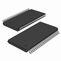
IC BUFFER 8OUTPUT DIFF 48-TSSOP
Manufacturer
IDT, Integrated Device Technology Inc
Type
Clock Bufferr
Series
-r
Datasheet
1.ICS9DB108BFLFT.pdf
(16 pages)
Specifications of ICS9DB108BGLF
Input
Clock
Output
Clock
Frequency - Max
220MHz
Voltage - Supply
3.135 V ~ 3.465 V
Operating Temperature
0°C ~ 70°C
Mounting Type
Surface Mount
Package / Case
48-TSSOP
Frequency-max
220MHz
Lead Free Status / RoHS Status
Lead free / RoHS Compliant
Other names
9DB108BGLF
Available stocks
Company
Part Number
Manufacturer
Quantity
Price
Company:

Part Number:
ICS9DB108BGLF
Manufacturer:
ICS
Quantity:
10
Company:
Part Number:
ICS9DB108BGLFT
Manufacturer:
SANYO
Quantity:
4 000


Absolute Max
0723G—12/02/08
T
1
2
3
Electrical Characteristics - Input/Supply/Common Output Parameters
Tambient
Operating Supply Current
Guaranteed by design and characterization, not 100% tested in production.
See timing diagrams for timing requirements.
Time from deassertion until outputs are >200 mV
ESD prot
Symbol
A
VDD_In
VDD_A
Modulation Frequency
Tcase
Tdrive_SRC_STOP#
= 0 - 70°C; Supply Voltage V
Powerdown Current
Input Capacitance
Input High Voltage
Input High Current
Input Low Voltage
Clk Stabilization
Input Low Current
V
V
Ts
Input Frequency
Pin Inductance
PLL Bandwidth
IH
IL
PARAMETER
Tdrive_PD#
Integrated
Circuit
Systems, Inc.
Trise
Tfall
3.3V Logic Supply Voltage
3.3V Core Supply Voltage
Ambient Operating Temp
Storage Temperature
1,2
Input ESD protection
1
3
human body model
Case Temperature
Input High Voltage
Input Low Voltage
1
Parameter
SYMBOL
I
I
DD3.3OP
DD3.3PD
T
C
BW
DD
L
C
V
V
I
I
STAB
I
F
IL1
IL2
OUT
IH
pin
IH
IN
IL
i
= 3.3 V +/-5%
V
From V
input clock stabilization or de-
IN
assertion of PD# to 1st clock
V
all differential pairs tri-stated
Full Active, C
IN
SRC_Stop# de-assertion
= 0 V; Inputs with no pull-up
Output pin capacitance
DIF output enable after
DIF output enable after
Triangular Modulation
= 0 V; Inputs with pull-up
PLL Bandwidth when
PLL Bandwidth when
Rise time of PD# and
Fall time of PD# and
all diff pairs driven
PD# de-assertion
DD
CONDITIONS
SRC_STOP#
SRC_STOP#
Logic Inputs
3.3 V +/-5%
3.3 V +/-5%
V
PLL_BW=0
PLL_BW=1
V
Power-Up and after
resistors
resistors
DD
IN
GND-0.5
= 3.3 V
= V
2000
Min
-65
L
0
= Full load;
DD
5
(Not recommended for new designs)
V
DD
Max
150
115
4.6
4.6
70
+0.5V
GND - 0.3
-200
MIN
1.5
80
30
-5
-5
2
100/133
166/200
Units
TYP
°C
°C
°
V
V
V
V
V
C
4
2
V
DD
MAX
250
220
300
0.8
60
12
33
10
5
7
5
6
1
5
5
+ 0.3
ICS9DB108
UNITS NOTES
MHz
MHz
MHz
kHz
mA
mA
mA
nH
ms
uA
uA
uA
pF
pF
ns
us
ns
ns
V
V
1,2
1,3
1,3
3
1
1
1
1
1
1
1
2
Related parts for ICS9DB108BGLF
Image
Part Number
Description
Manufacturer
Datasheet
Request
R

Part Number:
Description:
TRANSLATION DEVICE DPI 80-PQFP
Manufacturer:
IDT, Integrated Device Technology Inc
Datasheet:
Part Number:
Description:
IDT PART
Manufacturer:
IDT, Integrated Device Technology Inc
Datasheet:
Part Number:
Description:
IC LIU T1/E1/J1 OCTAL 256PBGA
Manufacturer:
IDT, Integrated Device Technology Inc
Datasheet:

Part Number:
Description:
IC FREQ TIMING GENERATOR 28TSSOP
Manufacturer:
IDT, Integrated Device Technology Inc
Datasheet:
Part Number:
Description:
IC CLK DVR PLL 1:10 40VFQFPN
Manufacturer:
IDT, Integrated Device Technology Inc
Datasheet:
Part Number:
Description:
IC CLK FANOUT BUFFER 1:18 32LQFP
Manufacturer:
IDT, Integrated Device Technology Inc
Datasheet:
Part Number:
Description:
IC CLK FANOUT BUFFER 1:18 32LQFP
Manufacturer:
IDT, Integrated Device Technology Inc
Datasheet:
Part Number:
Description:
IC CK505 VREG/RES 56TSSOP
Manufacturer:
IDT, Integrated Device Technology Inc
Datasheet:

Part Number:
Description:
IC SDRAM CLK DVR 1:10 48-TSSOP
Manufacturer:
IDT, Integrated Device Technology Inc
Datasheet:

Part Number:
Description:
IC CLK DVR PLL 1:10 48TSSOP
Manufacturer:
IDT, Integrated Device Technology Inc
Datasheet:
Part Number:
Description:
IC FLEXPC CLK PROGR P4 56-TSSOP
Manufacturer:
IDT, Integrated Device Technology Inc
Datasheet:
Part Number:
Description:
IC FLEXPC CLK PROGR P4 56-TSSOP
Manufacturer:
IDT, Integrated Device Technology Inc
Datasheet:
Part Number:
Description:
IC FLEXPC CLK PROGR P4 56-SSOP
Manufacturer:
IDT, Integrated Device Technology Inc
Datasheet:

Part Number:
Description:
IC PLL CLK DRIVER 2.5V 28-TSSOP
Manufacturer:
IDT, Integrated Device Technology Inc
Datasheet:
Part Number:
Description:
IC CLOCK DRIVER 2.5V 24-TSSOP
Manufacturer:
IDT, Integrated Device Technology Inc
Datasheet: