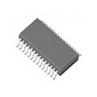
ICS9DB401BGLF IDT, Integrated Device Technology Inc, ICS9DB401BGLF Datasheet - Page 4

ICS9DB401BGLF
Manufacturer Part Number
ICS9DB401BGLF
Description
IC BUFFER 4OUTPUT DIFF 28-TSSOP
Manufacturer
IDT, Integrated Device Technology Inc
Type
Clock Buffer/Driverr
Datasheet
1.ICS9DB401BGLF.pdf
(16 pages)
Specifications of ICS9DB401BGLF
Input
Clock
Output
Clock
Frequency - Max
333.33MHz
Voltage - Supply
3.135 V ~ 3.465 V
Operating Temperature
0°C ~ 70°C
Mounting Type
Surface Mount
Package / Case
28-TSSOP
Frequency-max
333.33MHz
Number Of Elements
1
Supply Current
200mA
Pll Input Freq (min)
50MHz
Pll Input Freq (max)
200MHz
Operating Supply Voltage (typ)
3.3V
Operating Temp Range
0C to 70C
Package Type
TSSOP
Operating Supply Voltage (min)
3.135V
Operating Supply Voltage (max)
3.465V
Operating Temperature Classification
Commercial
Pin Count
28
Lead Free Status / RoHS Status
Lead free / RoHS Compliant
Other names
9DB401BGLF
Available stocks
Company
Part Number
Manufacturer
Quantity
Price
Part Number:
ICS9DB401BGLFT
Manufacturer:
ICS
Quantity:
20 000
The ICS9DB401 follows the Intel DB400 Differential Buffer Specification v2.0. This buffer provides four PCI-Express SRC
clocks. The ICS9DB401 is driven by a differential input pair from a CK409/CK410/CK410M main clock generator, such as the
ICS952601, ICS954101 or ICS954201. It provides ouputs meeting tight cycle-to-cycle jitter (50ps) and output-to-output skew
(50ps) requirements.
General Description
Block Diagram
Note: Polarities shown for OE_INV = 0.
Power Groups
1014B—09/07/06
5,11,18, 24
VDD
N/A
28
1
Integrated
Circuit
Systems, Inc.
Pin Number
SRC_IN
SRC_IN#
PD
BYPASS#/PLL
SDATA
SCLK
OE(3:0)
GND
4
27
27
4
4
CONTROL
LOGIC
Analog VDD & GND for PLL core
COMPATIBLE
SPREAD
SRC_IN/SRC_IN#
PLL
Description
DIF(1,2,5,6)
IREF
4
M
U
X
LOGIC
STOP
4
IREF
DIF(3:0))
ICS9DB401


