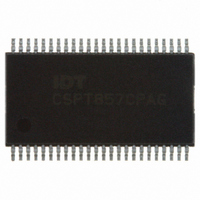
IDTCSPT857CPAG IDT, Integrated Device Technology Inc, IDTCSPT857CPAG Datasheet - Page 7

IDTCSPT857CPAG
Manufacturer Part Number
IDTCSPT857CPAG
Description
IC SDRAM CLK DVR 1:10 48-TSSOP
Manufacturer
IDT, Integrated Device Technology Inc
Type
PLL Clock Driverr
Datasheet
1.IDTCSPT857CNLG.pdf
(15 pages)
Specifications of IDTCSPT857CPAG
Input
Clock
Output
Differential
Frequency - Max
220MHz
Voltage - Supply
2.3 V ~ 2.7 V
Operating Temperature
0°C ~ 70°C
Mounting Type
Surface Mount
Package / Case
48-TSSOP
Frequency-max
220MHz
Lead Free Status / RoHS Status
Lead free / RoHS Compliant
Other names
800-1708
800-1708-5
800-1708
CSPT857CPAG
800-1708-5
800-1708
CSPT857CPAG
DC ELECTRICAL CHARACTERISTICS OVER OPERATING RANGE FOR PC3200
Following Conditions Apply Unless Otherwise Specified:
Commercial: T
TIMING REQUIREMENTS FOR PC1600 - PC2700
NOTES:
1.
2.
3. Application clock frequency is the range over which timing specifications apply.
4.
TIMING REQUIREMENTS FOR PC3200
NOTES:
1.
2.
3. Application clock frequency is the range over which timing specifications apply.
4.
NOTE:
1. V
IDTCSPT857C
2.5V - 2.6V PLL DIFFERENTIAL 1:10 SDRAM CLOCK DRIVER
V
V
Symbol
V
V
V
V
ID(DC) (1)
ID(AC) (1)
Symbol
Symbol
I
The PLL will track a spread spectrum clock input.
Operating clock frequency is the range over which the PLL will lock, but may not meet all timing specifications.
Stabilization time is the time required for the integrated PLL circuit to obtain phase lock of its feedback signal to its reference signal after power up.
V
DDPD
I
I
V
V
IL (dc)
IH (dc)
IL (ac)
IH (ac)
V
DDQ
ID
ADD
I
OH
IN
OL
f
f
IK
IX
CLK
t
CLK
t
DC
DC
is the magnitude of the difference between the input level on CLK and the input level on CLK.
t
t
L
L
Parameter
Input Clamp Voltage (All Inputs)
Static Input LOW Voltage
Static Input HIGH Voltage
Dynamic Input LOW Voltage
Dynamic Input HIGH Voltage
Output LOW Voltage
Output HIGH Voltage
Input Differential Cross Voltage
DC Input Differential Voltage
AC Input Differential Voltage
Input Current
Power-Down Current on V
Dynamic Power Supply Current on V
Dynamic Power Supply Current on A
A
= 0°C to +70°C; Industrial: T
Parameter
Operating Clock Frequency
Application Clock Frequency
Input Clock Duty Cycle
Stabilization Time
Parameter
Operating Clock Frequency
Application Clock Frequency
Input Clock Duty Cycle
Stabilization Time
(4)
(4)
DDQ
(1,2)
(1,2)
and A
(1,3)
(1,3)
A
= -40°C to +85°C
VDD
DDQ
VDD
Conditions
V
PWRDWN
PWRDWN
CLK, CLK, FBIN, FBIN
CLK, CLK, FBIN, FBIN
A
A
A
A
V
A
A
A
A
DDQ
VDD
VDD
VDD
VDD
DDQ
VDD
VDD
VDD
VDD
/V
/V
/V
/V
/V
/V
/V
/V
= 2.5V, I
= 2.7V, V
DDQ
DDQ
DDQ
DDQ
DDQ
DDQ
DDQ
DDQ
= Min., I
= Min., I
= Min., I
= Min., I
= Max., CLK = 0MHz or PWRDWN = L
= Max., CLK = 200MHz, 120Ω/14pF
= Max., CLK = 200MHz, 120Ω/14pF
= Max., CLK = 200MHz
I
I
= -18mA
= 0V to 2.7V
OH
OL
OL
OH
7
= 100μA
= 12mA
= -100μA
= -12mA
COMMERCIAL AND INDUSTRIAL TEMPERATURE RANGES
Min.
Min.
⎯
⎯
60
60
60
60
40
40
V
V
DDQ
DDQ
– 0.3
Min.
0.36
⎯
1.7
⎯
1.7
⎯
⎯
1.7
0.7
⎯
⎯
⎯
⎯
/2 – 0.2
– 0.1
Typ.
Max.
Max.
100
320
250
200
200
100
220
220
100
⎯
⎯
⎯
⎯
60
60
V
V
V
V
DDQ
DDQ
DDQ
DDQ
V
Max.
– 1.2
±10
200
360
300
0.7
0.7
0.1
0.6
DDQ
12
/2 + 0.2
+ 0.3
+ 0.6
+ 0.6
MHz
MHz
MHz
MHz
Unit
Unit
μs
μs
%
%
Unit
μA
μA
mA
mA
V
V
V
V
V
V
V
V


