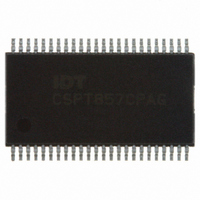
IDTCSPT857CPAG IDT, Integrated Device Technology Inc, IDTCSPT857CPAG Datasheet - Page 5

IDTCSPT857CPAG
Manufacturer Part Number
IDTCSPT857CPAG
Description
IC SDRAM CLK DVR 1:10 48-TSSOP
Manufacturer
IDT, Integrated Device Technology Inc
Type
PLL Clock Driverr
Datasheet
1.IDTCSPT857CNLG.pdf
(15 pages)
Specifications of IDTCSPT857CPAG
Input
Clock
Output
Differential
Frequency - Max
220MHz
Voltage - Supply
2.3 V ~ 2.7 V
Operating Temperature
0°C ~ 70°C
Mounting Type
Surface Mount
Package / Case
48-TSSOP
Frequency-max
220MHz
Lead Free Status / RoHS Status
Lead free / RoHS Compliant
Other names
800-1708
800-1708-5
800-1708
CSPT857CPAG
800-1708-5
800-1708
CSPT857CPAG
PIN DESCRIPTION (TSSOP/TVSOP)
RECOMMENDED OPERATING CONDITIONS
PIN DESCRIPTION (VFBGA)
PIN DESCRIPTION (MLF)
IDTCSPT857C
2.5V - 2.6V PLL DIFFERENTIAL 1:10 SDRAM CLOCK DRIVER
Symbol
AV
V
FBOUT, FBOUT
FBOUT, FBOUT
FBOUT, FBOUT
DDQ
T
A
DD
FBIN, FBIN
FBIN, FBIN
FBIN, FBIN
PWRDWN
Pin Name
CLK, CLK
PWRDWN
Pin Name
CLK, CLK
PWRDWN
Pin Name
CLK, CLK
AGND
AGND
AGND
AV
GND
V
AV
Y
Y
AV
GND
GND
V
V
Y
Y
Y
Y
DDQ
[0:9]
[0:9]
DDQ
DDQ
[0:9]
[0:9]
[0:9]
[0:9]
DD
DD
DD
Supply Voltage
I/O Supply Voltage
Operating Free-Air Temperature
A3, A4, C1, C2, C5, C6, H2, H5, K3, K4
A1, A6, B2, B5, D1, D6, J2, J5, K1, K6
A2, A5, B1, B6, D2, D5, J1, J6, K2, K5
3, 12, 14, 17, 19, 29, 32, 34, 37, 39
2, 11, 15, 16, 20, 30, 31, 35, 36, 40
3, 5, 10, 20, 22, 27, 29, 39, 44, 46
1, 7, 8, 18, 24, 25, 31, 41, 42, 48
2, 6, 9, 19, 23, 26, 30, 40, 43, 47
4, 11, 12, 15, 21, 28, 34, 38, 45
B3, B4, E1, E2, E5, G1, G6, J3, J4
4, 7, 13, 18, 23, 24, 28, 33, 38
Pin Number
Pin Number
Parameter
Pin Number
13, 14
35, 36
32, 33
25, 26
21, 22
1, 10
5, 6
H6, G5
17
16
37
27
F1, F2
F5, F6
9
8
PC1600-PC2700
PC3200
H1
G2
E6
Ground for analog supply
Analog supply
Differential clock input
Feedback differential clock input
Feedback differential clock output
Ground
Output enable for Y and Y
I/O supply
Buffered output of input clock, CLK
Buffered output of input clock, CLK
Buffered output of input clock, CLK
Ground for analog supply
Analog supply
Differential clock input
Feedback differential clock input
Feedback differential clock output
Ground
Output enable for Y and Y
I/O supply
Buffered output of input clock, CLK
Buffered output of input clock, CLK
Buffered output of input clock, CLK
Ground for analog supply
Analog supply
Differential clock input
Feedback differential clock input
Feedback differential clock output
Ground
Output enable for Y and Y
I/O supply
V
5
DDQ
Min.
2.3
2.5
-40
– 0.12
COMMERCIAL AND INDUSTRIAL TEMPERATURE RANGES
Description
Description
Description
Typ.
V
2.5
2.6
⎯
DDQ
Max.
+85
2.7
2.7
2.7
Unit
°
V
V
C


