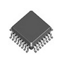
87946AYI-147 IDT, Integrated Device Technology Inc, 87946AYI-147 Datasheet

87946AYI-147
Specifications of 87946AYI-147
Available stocks
Related parts for 87946AYI-147
87946AYI-147 Summary of contents
Page 1
... Pulldown DIV_SELB Pulldown DIV_SELC Pulldown MR/nOE ICS87946AYI-147 REVISION A AUGUST 7, 2009 Features • Ten single ended LVCMOS/LVTTL outputs, 7Ω typical output impedance • Selectable LVCMOS/LVTTL CLK0 and CLK1 inputs • CLK0 and CLK1 can accept the following input levels: LVCMOS and LVTTL • ...
Page 2
... Input Pullup Resistor PULLUP R Input Pulldown Resistor PULLDOWN R Output Impedance OUT ICS87946AYI-147 REVISION A AUGUST 7, 2009 Type Description Clock select input. When HIGH, selects CLK1. Pulldown When LOW, selects CLK0. LVCMOS / LVTTL interface levels. Positive supply pin. Pullup Single-ended clock inputs. LVCMOS/LVTTL interface levels. ...
Page 3
... STG DC Electrical Characteristics Table 4A. Power Supply DC Characteristics, V Symbol Parameter V Positive Supply Voltage Output Supply Voltage DDA, DDB, DDC I Power Supply Current Output Supply Current DDA DDB DDC ICS87946AYI-147 REVISION A AUGUST 7, 2009 DIV_SELC QA0:QA2 X X High-Impedance Active 1 X Active X 0 Active X 1 Active Rating 4 ...
Page 4
... DIV_SELC, CLK_SEL IL Current CLK0, CLK1 V Output High Voltage; NOTE Output Low Voltage; NOTE Output Hi-Z Current Low OZL I Output Hi-Z Current High OZH Ω NOTE 1: Outputs terminated with 50 ICS87946AYI-147 REVISION A AUGUST 7, 2009 = 3.3V ± 5 DDA Test Conditions = DDA DDB Test Conditions 3. ...
Page 5
... Low DIV_SELC, CLK_SEL IL Current CLK0, CLK1 Output High Voltage NOTE 1 V Output Low Voltage; NOTE Output Hi-Z Current Low OZL I Output Hi-Z Current High OZH Ω NOTE 1: Outputs terminated with 50 ICS87946AYI-147 REVISION A AUGUST 7, 2009 = 3.3V ± 5 Test Conditions 3.465V 3.465V 3.465V ...
Page 6
... NOTE 5: Defined as skew between outputs on different devices operating at the same supply voltage and with equal load conditions. Using the same type of inputs on each device, the outputs are measured at V NOTE 6: These parameters are guaranteed by characterization. Not tested in production. NOTE 7: This parameter is defined in accordance with JEDEC Standard 65. ICS87946AYI-147 REVISION A AUGUST 7, 2009 = 3.3V ± ...
Page 7
... NOTE 5: Defined as skew between outputs on different devices operating at the same supply voltage and with equal load conditions. Using the same type of inputs on each device, the outputs are measured at V NOTE 6: These parameters are guaranteed by characterization. Not tested in production. NOTE 7: This parameter is defined in accordance with JEDEC Standard 65. ICS87946AYI-147 REVISION A AUGUST 7, 2009 = 3.3V ± 5 ...
Page 8
... V DDO Qy 2 tsk(o) Output Skew V DDx 2 QX0:QXx V DDx 2 QX0:QXx tsk(b) Where X = Bank Bank Skew ICS87946AYI-147 REVISION A AUGUST 7, 2009 2.05V± 5% SCOPE LVCMOS 3.3V Core/2.5V Output Load AC Test Circuit Part 1 Qx Part 2 Qy Part-to-Part Skew QBx, QCx QAx Multiple Frequency Skew 8 LOW SKEW, ÷1, ÷2 LVCMOS/LVTTL CLOCK GENERATOR 1.25V± ...
Page 9
... QBx, QCx PERIOD t PW odc = t PERIOD t & PERIOD 80% QAx, 20% QBx, QCx t R Output Rise/Fall Time ICS87946AYI-147 REVISION A AUGUST 7, 2009 V V DDx DDx 2 2 CLK0, CLK1 Propagation Delay 80% 20 LOW SKEW, ÷1, ÷2 LVCMOS/LVTTL CLOCK GENERATOR V DDx 2 V QAx, DDx 2 QBx, QCx ...
Page 10
... NOTE: Most modern PCB designs use multi-layered boards. The data in the second row pertains to most designs. Transistor Count The transistor count for ICS87946I-147 is: 1204 Pin compatible to the MPC9446 and MPC946 ICS87946AYI-147 REVISION A AUGUST 7, 2009 LOW SKEW, ÷1, ÷2 LVCMOS/LVTTL CLOCK GENERATOR O puts: ...
Page 11
... Basic D2 & E2 5.60 Ref. e 0.80 Basic L 0.45 0.60 θ 0° ccc Reference Document: JEDEC Publication 95, MS-026 ICS87946AYI-147 REVISION A AUGUST 7, 2009 Maximum 1.60 0.15 1.45 0.45 0.20 0.75 7° 0.10 11 LOW SKEW, ÷1, ÷2 LVCMOS/LVTTL CLOCK GENERATOR ©2009 Integrated Device Technology, Inc. ...
Page 12
... IDT. IDT reserves the right to change any circuitry or specifications without notice. IDT does not authorize or warrant any IDT product for use in life support devices or critical medical instruments. ICS87946AYI-147 REVISION A AUGUST 7, 2009 LOW SKEW, ÷1, ÷2 LVCMOS/LVTTL CLOCK GENERATOR Package ...
Page 13
... T5A - T5B ICS87946AYI-147 REVISION A AUGUST 7, 2009 Description of Change Features section added Lead-Free bullet. Pin Description Table - corrected description for V Parameter Measurement Information Section - added part-to-part skew, bank skew, and multiple frequency skew diagrams. Application Section - added Recommendations for Unused Input and Output Pins ...
Page 14
ICS87946I-147 Data Sheet 6024 Silver Creek Valley Road Sales 800-345-7015 (inside USA) San Jose, California 95138 +408-284-8200 (outside USA) Fax: 408-284-2775 www.IDT.com/go/contactIDT DISCLAIMER Integrated Device Technology, Inc. (IDT) and its subsidiaries reserve the right to modify the products and/or specifications ...


