SPB11N60C3XT Infineon Technologies, SPB11N60C3XT Datasheet
SPB11N60C3XT
Specifications of SPB11N60C3XT


Related parts for SPB11N60C3XT

SPB11N60C3XT Summary of contents
Page 1
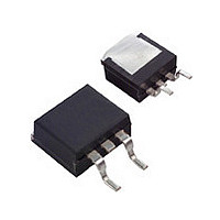
Cool MOS™ Power Transistor Feature • New revolutionary high voltage technology • Ultra low gate charge • Periodic avalanche rated • Extreme dv/dt rated • High peak current capability • Improved transconductance Type Package SPB11N60C3 PG-TO263 Maximum Ratings Parameter Continuous ...
Page 2
Maximum Ratings Parameter Drain Source voltage slope = 480 125 ° Thermal Characteristics Parameter Thermal resistance, junction - case Thermal resistance, junction - ambient, leaded SMD version, device on ...
Page 3
Electrical Characteristics Parameter Transconductance Input capacitance Output capacitance Reverse transfer capacitance Effective output capacitance, energy related Effective output capacitance, time related Turn-on delay time Rise time Turn-off delay time Fall time Gate Charge Characteristics Gate to source charge Gate to ...
Page 4
Electrical Characteristics Parameter Inverse diode continuous forward current Inverse diode direct current, pulsed Inverse diode forward voltage Reverse recovery time Reverse recovery charge Peak reverse recovery current Peak rate of fall of reverse recovery current Typical Transient Thermal Characteristics Symbol ...
Page 5
Power dissipation tot C SPP11N60C3 140 W 120 110 100 Safe operating area ...
Page 6
Transient thermal impedance thJC p parameter K Typ. ...
Page 7
Typ. drain-source on resistance R =f(I ) DS(on) D parameter: T =150° Ω 4. 1.6 1.4 1.2 1 0.8 0.6 0 Typ. transfer characteristics ≥ 2 ...
Page 8
Forward characteristics of body diode parameter µ SPP11N60C3 °C typ 150 °C ...
Page 9
Typ. drain source voltage slope dv/dt = f(R ), inductive load par.: V =380V, V =0/+13V 140 V/ns dv/dt(off) 120 110 100 dv/dt(on ...
Page 10
Avalanche energy par 5 350 mJ 250 200 150 100 100 23 Avalanche power losses P = ...
Page 11
Typ. C stored energy oss E =f(V ) oss DS 7.5 µJ 6 5.5 5 4.5 4 3.5 3 2.5 2 1 100 200 300 Definition of diodes switching characteristics Rev. 2.6 400 600 V ...
Page 12
PG-TO263 Rev. 2.6 Page 12 SPB11N60C3 2007-12-14 ...
Page 13
... Infineon Technologies Office. Infineon Technologies components may be used in life-support devices or systems only with the express written approval of Infineon Technologies failure of such components can reasonably be expected to cause the failure of that life-support device or system or to affect the safety or effectiveness of that device or system ...