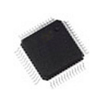
PSD834F2V10MI STMicroelectronics, PSD834F2V10MI Datasheet - Page 80

PSD834F2V10MI
Manufacturer Part Number
PSD834F2V10MI
Description
Manufacturer
STMicroelectronics
Datasheet
1.PSD834F2V10MI.pdf
(95 pages)
Specifications of PSD834F2V10MI
Operating Temperature (max)
85C
Operating Temperature (min)
-40C
Operating Temperature Classification
Industrial
Package Type
PQFP
Mounting
Surface Mount
Pin Count
52
Lead Free Status / RoHS Status
Compliant
- Current page: 80 of 95
- Download datasheet (816Kb)
PSD834F2V
Table 48. WRITE Timing
Note: 1. Any input used to select an internal PSD function.
80/95
t
t
t
t
t
t
t
t
t
t
t
t
t
t
Symbol
LVLX
AVLX
LXAX
AVWL
SLWL
DVWH
WHDX
WLWH
WHAX1
WHAX2
WHPV
DVMV
AVPV
WLMV
2. In multiplexed mode, latched address generated from ADIO delay to address output on any port.
3. WR has the same timing as E, LDS, UDS, WRL, and WRH signals.
4. Assuming data is stable before active WRITE signal.
5. Assuming WRITE is active before data becomes valid.
6. TWHAX2 is the address hold time for DPLD inputs that are used to generate Sector Select signals for internal PSD memory.
ALE or AS Pulse Width
Address Setup Time
Address Hold Time
Address Valid to Leading
Edge of WR
CS Valid to Leading Edge of WR
WR Data Setup Time
WR Data Hold Time
WR Pulse Width
Trailing Edge of WR to Address Invalid
Trailing Edge of WR to DPLD Address
Invalid
Trailing Edge of WR to Port Output
Valid Using I/O Port Data Register
Data Valid to Port Output Valid
Using Macrocell Register Preset/Clear
Address Input Valid to Address
Output Delay
WR Valid to Port Output Valid Using
Macrocell Register Preset/Clear
Parameter
Conditions
(Notes
(Notes
(Notes
(Note
(Note
(Note
(Note
(Note
(Note
(Note
(Note
(Note
(Note
3,6
1,3
3,5
3,4
1
1
3
3
3
3
3
3
2
)
)
)
)
)
)
)
)
)
)
)
)
)
Min Max Min Max Min Max
26
17
17
45
46
10
9
9
7
0
-10
33
70
33
70
26
10
12
20
20
45
48
12
8
0
-15
35
70
35
70
30
12
14
25
25
50
10
53
17
0
-20
40
80
40
80
Unit
ns
ns
ns
ns
ns
ns
ns
ns
ns
ns
ns
ns
ns
Related parts for PSD834F2V10MI
Image
Part Number
Description
Manufacturer
Datasheet
Request
R

Part Number:
Description:
Flash In-System Programmable (ISP) Peripherals for 8-bit MCUs, 5V
Manufacturer:
STMicroelectronics
Datasheet:

Part Number:
Description:
IC FLASH 2MBIT 90NS 52PLCC
Manufacturer:
STMicroelectronics
Datasheet:

Part Number:
Description:
IC FLASH 2MBIT 70NS 52QFP
Manufacturer:
STMicroelectronics
Datasheet:

Part Number:
Description:
IC FLASH 2MBIT 90NS 52QFP
Manufacturer:
STMicroelectronics
Datasheet:

Part Number:
Description:
IC FLASH 2MBIT 70NS 52PLCC
Manufacturer:
STMicroelectronics
Datasheet:

Part Number:
Description:
IC FLASH 2MBIT 90NS 52PLCC
Manufacturer:
STMicroelectronics
Datasheet:

Part Number:
Description:
IC FLASH 2MBIT 90NS 52QFP
Manufacturer:
STMicroelectronics
Datasheet:

Part Number:
Description:
Manufacturer:
STMicroelectronics
Datasheet:

Part Number:
Description:
Manufacturer:
STMicroelectronics
Datasheet:

Part Number:
Description:
Three Phase Rectifier Bridge
Manufacturer:
POWERSEM [Powersem GmbH]
Datasheet:

Part Number:
Description:
STMicroelectronics [RIPPLE-CARRY BINARY COUNTER/DIVIDERS]
Manufacturer:
STMicroelectronics
Datasheet:

Part Number:
Description:
STMicroelectronics [LIQUID-CRYSTAL DISPLAY DRIVERS]
Manufacturer:
STMicroelectronics
Datasheet:

Part Number:
Description:
BOARD EVAL FOR MEMS SENSORS
Manufacturer:
STMicroelectronics
Datasheet:


