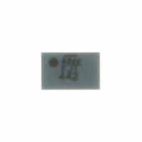
EMIF02-MIC02F2 STMicroelectronics, EMIF02-MIC02F2 Datasheet

EMIF02-MIC02F2
Specifications of EMIF02-MIC02F2
Available stocks
Related parts for EMIF02-MIC02F2
EMIF02-MIC02F2 Summary of contents
Page 1
... This filter includes an ESD protection circuitry which prevents the device from destruction when subjected to ESD surges up 15 kV. April 2008 2-line IPAD™, EMI filter and ESD protection Figure 1. Figure 2. Input GND TM: IPAD is a trademark of STMicroelectronics. Rev 3 EMIF02-MIC02F2 Flip Chip (6 bumps) Pin configuration (bump side GND ...
Page 2
... I Peak pulse current PP Series resistance between input and R I/O output C Input capacitance per line line Symbol I line 2 °C) amb Parameter = 25 °C) amb Parameters RM Test conditions = 12 V per line EMIF02-MIC02F2 Value 125 -40 to +85 -55 to 150 Min Typ Max 14 16 500 423 ...
Page 3
... EMIF02-MIC02F2 Figure 3. S21 (dB) attenuation measurement and Aplac simulation - 10. 15.00 - 20.00 - 25.00 - 30.00 - 35.00 - 40.00 - 45.00 - 50.00 1.0M 3.0M 10.0M 30.0M 100.0M 300.0M f/Hz Figure 5. Digital crosstalk measurement Figure 7. ESD response to IEC61000-4-2 (+15 kV air discharge) on one input V(in) and on one output (Vout) Figure 4 ...
Page 4
... IKF = 1000 IKF = 1000 IS = 10f IS = 10f ISR = 100p ISR = 100p 0.3333 M = 0.3333 RS = Rs_int RS = Rs_gnd 50n TT = 50n EMIF02-MIC02F2 gnd 50pH 50m Lgnd Cgnd Cgnd Rgnd Ls 400pH Rs 100m R_470R 482.6 Cz_ext 8.73pF Rs_ext 850m Cz_int 2.9pF Rs_int 850m Cz_gnd 215.61pF Rs_gnd 470m ...
Page 5
... EMIF02-MIC02F2 3 Ordering information scheme Figure 11. Ordering information scheme EMI Filter Number of lines Information x = resistance value (Ohms capacitance value / letters = application 2 digits = version Package F = Flip Chip Lead-free, pitch = 500 µm, bump = 315 µm 4 Package information In order to meet environmental requirements, ST offers these devices in ECOPACK packages ...
Page 6
... AN1751: “EMI filters: Recommendations and measurements” 6/8 Figure 14. Marking Dot identifying Pin A1 location 0.73 ± 0.05 User direction of unreeling All dimensions in mm Marking Package FJ Flip Chip EMIF02-MIC02F2 Dot, ST logo xx = marking z = manufacturing location yww = datecode (y = year ww = week Ø 1.5 ± 0.1 4 ± ...
Page 7
... EMIF02-MIC02F2 6 Revision history Table 4. Document revision history Date 12-Oct-2004 11-Jan-2006 17-Apr-2008 Revision 1 Initial release. ECOPACK statement added. Die dimensions modified in 2 and first page. Typographical errors corrected. Updated ECOPACK statement. Updated 3 Figure 15. Reformatted to current standards. Revision history Changes Figure 12. Figure 11, ...
Page 8
... Australia - Belgium - Brazil - Canada - China - Czech Republic - Finland - France - Germany - Hong Kong - India - Israel - Italy - Japan - Malaysia - Malta - Morocco - Singapore - Spain - Sweden - Switzerland - United Kingdom - United States of America 8/8 Please Read Carefully: © 2008 STMicroelectronics - All rights reserved STMicroelectronics group of companies www.st.com EMIF02-MIC02F2 ...


