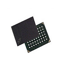
MT48H4M16LFB4-75 IT:H Micron Technology Inc, MT48H4M16LFB4-75 IT:H Datasheet - Page 7

MT48H4M16LFB4-75 IT:H
Manufacturer Part Number
MT48H4M16LFB4-75 IT:H
Description
Manufacturer
Micron Technology Inc
Type
SDRAMr
Datasheet
1.MT48H4M16LFB4-75_ITH.pdf
(62 pages)
Specifications of MT48H4M16LFB4-75 IT:H
Organization
4Mx16
Density
64Mb
Address Bus
14b
Maximum Clock Rate
133MHz
Operating Supply Voltage (typ)
1.8V
Package Type
VFBGA
Operating Temp Range
-40C to 85C
Operating Supply Voltage (max)
1.9V
Operating Supply Voltage (min)
1.7V
Supply Current
50mA
Pin Count
54
Mounting
Surface Mount
Operating Temperature Classification
Industrial
Lead Free Status / RoHS Status
Compliant
Table 3:
PDF: 09005aef8237ed98/Source: 09005aef8237ed68
64mb_x16_Mobile SDRAM_Y24L_2.fm - Rev. C 10/07 EN
H7, H8, J8, J7, J3, J2, H3,
A8, B9, B8, C9, C8, D9,
D8, E9, E1, D2, D1, C2,
H2, H1, G3, H9, G2
54-Ball VFBGA
A7, B3, C7, D3
A3, B7, C3, D7
C1, B2, B1, A2
A9, E7, J9
A1, E3, J1
F7, F8, F9
G7, G8
E2, G1
E8, F1
G9
F2
F3
Ball Descriptions
CAS#, RAS#,
DQ0–DQ15
BA0, BA1
Symbol
A0–A11
LDQM,
UDQM
V
V
WE#
CKE
V
CLK
CS#
V
NC
DD
SS
DD
SS
Q
Q
Supply DQ power: Provides isolated power to DQ for improved noise immunity.
Supply DQ ground: Provides isolated ground to DQ for improved noise immunity.
Supply Core power supply.
Supply Ground.
Input
Input
Input
Input
Input
Input
Input
Type
I/O
–
Description
Clock: CLK is driven by the system clock. All SDRAM input signals are
sampled on the positive edge of CLK. CLK also increments the internal
burst counter and controls the output registers.
Clock enable: CKE activates (HIGH) and deactivates (LOW) the CLK signal.
Deactivating the clock provides precharge power-down and SELF REFRESH
operation (all banks idle), ACTIVE POWER-DOWN (row active in any
bank), deep power-down (all banks idle), or CLOCK SUSPEND operation
(burst/access in progress). CKE is synchronous except after the device
enters power-down and self refresh modes, where CKE becomes
asynchronous until after exiting the same mode. The input buffers,
including CLK, are disabled during power-down and self refresh modes,
providing low standby power. CKE may be tied HIGH.
Chip select: CS# enables (registered LOW) and disables (registered HIGH)
the command decoder. All commands are masked when CS# is registered
HIGH. CS# provides for external bank selection on systems with multiple
banks. CS# is considered part of the command code.
Command inputs: CAS#, RAS#, and WE# (along with CS#) define the
command being entered.
Input/output mask: DQM is sampled HIGH and is an input mask signal for
write accesses and an output enable signal for read accesses. Input data is
masked during a WRITE cycle. The output buffers are placed in a High-Z
state (two-clock latency) during a READ cycle. LDQM corresponds to DQ0–
DQ7, UDQM corresponds to DQ8–DQ15. LDQM and UDQM are considered
same state when referenced as DQM. DQM loading is designed to match
that of DQ balls.
Bank address input(s): BA0 and BA1 define to which bank the ACTIVE,
READ, WRITE, or PRECHARGE command is being applied. These pins also
select between the mode register and the extended mode register.
Address inputs: A0–A11 are sampled during the ACTIVE command (row-
address A0–A11) and READ/WRITE command (column-address A0–A7;
with A10 defining auto precharge) to select one location out of the
memory array in the respective bank. A10 is sampled during a
PRECHARGE command to determine whether all banks are to be
precharged (A10 HIGH) or bank selected by BA0, BA1. The address inputs
also provide the op-code during a LOAD MODE REGISTER command.
Data input/output: Data bus.
NC = no connect (internally unconnected): These may be left
unconnected, but it is recommended that they be connected to V
DNU = do not use; must be left unconnected.
7
Micron Technology, Inc., reserves the right to change products or specifications without notice.
64Mb: 4 Meg x 16 Mobile SDRAM
General Description
©2006 Micron Technology, Inc. All rights reserved.
SS
.


