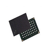
MT48H4M16LFB4-75 IT:H Micron Technology Inc, MT48H4M16LFB4-75 IT:H Datasheet - Page 31

MT48H4M16LFB4-75 IT:H
Manufacturer Part Number
MT48H4M16LFB4-75 IT:H
Description
Manufacturer
Micron Technology Inc
Type
SDRAMr
Datasheet
1.MT48H4M16LFB4-75_ITH.pdf
(62 pages)
Specifications of MT48H4M16LFB4-75 IT:H
Organization
4Mx16
Density
64Mb
Address Bus
14b
Maximum Clock Rate
133MHz
Operating Supply Voltage (typ)
1.8V
Package Type
VFBGA
Operating Temp Range
-40C to 85C
Operating Supply Voltage (max)
1.9V
Operating Supply Voltage (min)
1.7V
Supply Current
50mA
Pin Count
54
Mounting
Surface Mount
Operating Temperature Classification
Industrial
Lead Free Status / RoHS Status
Compliant
Burst Read/Single Write
Concurrent Auto Precharge
READ with Auto Precharge
Figure 27:
PDF: 09005aef8237ed98/Source: 09005aef8237ed68
64mb_x16_Mobile SDRAM_Y24L_2.fm - Rev. C 10/07 EN
READ with Auto Precharge Interrupted by a READ
Note:
1. Interrupted by a READ (with or without auto precharge): A READ to bank m will inter-
2. Interrupted by a WRITE (with or without auto precharge): When a WRITE to bank m
The burst read/single write mode is entered by programming the write burst mode bit
(M9) in the mode register to a logic 1. In this mode, all WRITE commands result in the
access of a single column location (burst of one), regardless of the programmed burst
length. READ commands access columns according to the programmed burst length
and sequence, just as in the normal mode of operation (M9 = 0).
Micron SDRAM devices support concurrent auto precharge, which enables an access
command (READ or WRITE) to another bank while an access command with auto
precharge enabled is executing. Four cases where concurrent auto precharge occurs are
defined below.
Internal
States
rupt a READ on bank n, two or three clocks later, depending on CL. The precharge to
bank n will begin when the READ to bank m is registered (see Figure 27).
registers, a READ on bank n will be interrupted. DQM should be used two clocks prior
to the WRITE command to prevent bus contention. The precharge to bank n will
begin when the WRITE to bank m is registered (see Figure 28 on page 32).
DQM is LOW.
Command
Bank m
Address
Bank n
CLK
DQ
Page active
T0
NOP
READ - AP
Bank n,
Page active
Bank n
Col a
T1
READ with BL = 4
31
CL = 3 (Bank n)
T2
NOP
Micron Technology, Inc., reserves the right to change products or specifications without notice.
Bank m,
READ - AP
T3
Bank m
Col d
Interrupt burst, precharge
READ with BL = 4
64Mb: 4 Meg x 16 Mobile SDRAM
Transitioning Data
T4
CL = 3 (Bank m)
NOP
D
OUT
a
t
RP - Bank n
T5
NOP
D
a + 1
OUT
©2006 Micron Technology, Inc. All rights reserved.
T6
NOP
D
OUT
d
Don’t Care
Idle
T7
NOP
t RP - Bank m
Precharge
D
Operations
d + 1
OUT


