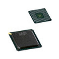
SAA7118E/V1/M5.557 NXP Semiconductors, SAA7118E/V1/M5.557 Datasheet - Page 77

SAA7118E/V1/M5.557
Manufacturer Part Number
SAA7118E/V1/M5.557
Description
Manufacturer
NXP Semiconductors
Datasheet
1.SAA7118EV1M5.557.pdf
(177 pages)
Specifications of SAA7118E/V1/M5.557
Adc/dac Resolution
9b
Screening Level
Commercial
Package Type
LBGA
Pin Count
156
Lead Free Status / RoHS Status
Compliant
- Current page: 77 of 177
- Download datasheet (972Kb)
NXP Semiconductors
SAA7118_7
Product data sheet
9.5.2 X port configured as input
9.6 Image port (I port)
Table 32.
If the data input mode is selected at the expansion port, then the scaler can select its input
data stream from the on-chip video decoder, or from the expansion port (controlled by bit
SCSRC[1:0] 91h[5:4]). Byte serial Y-C
schemes, or raw samples from an external ADC may be input (see also bits FSC[2:0]
91h[2:0]). The input stream must be accompanied by an external clock (XCLK), qualifier
XDQ and reference signals XRH and XRV. Instead of the reference signal, embedded
SAV and EAV codes according to ITU 656 are also accepted. The protection bits are not
evaluated.
XRH and XRV carry the horizontal and vertical synchronization signals for the digital
video stream through the expansion port. The field ID of the input video stream is carried
in the phase (edge) of XRV and state of XRH, or directly as FS (frame sync, odd/even
signal) on the XRV pin (controlled by XFDV[92h[7]], XFDH[92h[6]] and XDV[1:0] 92h[5:4]).
The trigger events on XRH (rising/falling edge) and XRV (rising/falling/both edges) for the
scalers acquisition window are defined by XDV[1:0] 92h[5:4] and XDH[92h[2]]. The signal
polarity of the qualifier can also be defined (bit XDQ[92h[1]]). Alternatively to a qualifier,
the input clock can be applied to a gated clock (clock gated with a data qualifier, controlled
by bit XCKS[92h[0]]). In this event, all input data will be qualified.
As the VBI data slicer may have different requirements for its input reference signals from
X port XRV, XRH, XDQ, XCLK and XPD7 to XPD0, a second set of parameters is
available for defining the meaning of the X port input signals and polarities for the VBI data
slicer input path. These bits are defined in subaddresses 81h and 82h.
The image port transfers data from the scaler as well as from the VBI data slicer, if
selected (maximum 33 MHz). The reference clock is available at the ICLK pin, as an
output, or as an input (maximum 33 MHz). As output, ICLK is derived from the line-locked
decoder or expansion port input clock. The data stream from the scaler output is normally
discontinuous. Therefore valid data during a clock cycle is accompanied by a data
qualifying (data valid) flag on pin IDQ. For pin constrained applications the IDQ pin can be
programmed to function as a gated clock output (bit ICKS2[80h[2]]).
Line number
1 to 22
23
24 to 309
310
311 and 312
313 to 335
336
337 to 622
623
624 and 625
625 lines/50 Hz vertical timing
F (ITU 656)
0
0
0
0
0
1
1
1
1
1
Rev. 07 — 7 July 2008
V
OFTS[2:0] = 000
(ITU 656)
1
0
0
0
1
1
0
0
0
1
Multistandard video decoder with adaptive comb filter
B
-C
R
4 : 2 : 2, or subsets for other sampling
OFTS[1:0] = 10
according to selected VGATE position
type via VSTA and VSTO
(subaddresses 15h to 17h);
see
Table 60
to
Table 62
SAA7118
© NXP B.V. 2008. All rights reserved.
77 of 177
Related parts for SAA7118E/V1/M5.557
Image
Part Number
Description
Manufacturer
Datasheet
Request
R
Part Number:
Description:
Video ICs COMPONENT + VIDEO PROCESSOR
Manufacturer:
NXP Semiconductors

Part Number:
Description:
IC VIDEO DECOD W/FILTER 156LBGA
Manufacturer:
NXP Semiconductors
Datasheet:
Part Number:
Description:
IC VIDEO DECOD W/FILTER 156LBGA
Manufacturer:
NXP Semiconductors

Part Number:
Description:
IC VIDEO DECODER W/FILTER 156BGA
Manufacturer:
NXP Semiconductors

Part Number:
Description:
IC VIDEO DECODR W/FILTER 156LBGA
Manufacturer:
NXP Semiconductors

Part Number:
Description:
IC VIDEO DECODR W/FILTER 156LBGA
Manufacturer:
NXP Semiconductors
Part Number:
Description:
Video ICs VIDEO DECODER W/FILTER
Manufacturer:
NXP Semiconductors

Part Number:
Description:
Video ICs COMPONENT VID DECODER W/COMB F
Manufacturer:
NXP Semiconductors
Datasheet:

Part Number:
Description:
Manufacturer:
NXP Semiconductors
Datasheet:
Part Number:
Description:
NXP Semiconductors designed the LPC2420/2460 microcontroller around a 16-bit/32-bitARM7TDMI-S CPU core with real-time debug interfaces that include both JTAG andembedded trace
Manufacturer:
NXP Semiconductors
Datasheet:

Part Number:
Description:
NXP Semiconductors designed the LPC2458 microcontroller around a 16-bit/32-bitARM7TDMI-S CPU core with real-time debug interfaces that include both JTAG andembedded trace
Manufacturer:
NXP Semiconductors
Datasheet:
Part Number:
Description:
NXP Semiconductors designed the LPC2468 microcontroller around a 16-bit/32-bitARM7TDMI-S CPU core with real-time debug interfaces that include both JTAG andembedded trace
Manufacturer:
NXP Semiconductors
Datasheet:
Part Number:
Description:
NXP Semiconductors designed the LPC2470 microcontroller, powered by theARM7TDMI-S core, to be a highly integrated microcontroller for a wide range ofapplications that require advanced communications and high quality graphic displays
Manufacturer:
NXP Semiconductors
Datasheet:


