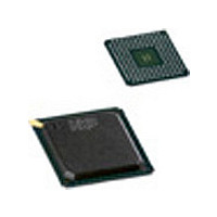
SAA7118E/V1/M5.557 NXP Semiconductors, SAA7118E/V1/M5.557 Datasheet - Page 154

SAA7118E/V1/M5.557
Manufacturer Part Number
SAA7118E/V1/M5.557
Description
Manufacturer
NXP Semiconductors
Datasheet
1.SAA7118EV1M5.557.pdf
(177 pages)
Specifications of SAA7118E/V1/M5.557
Adc/dac Resolution
9b
Screening Level
Commercial
Package Type
LBGA
Pin Count
156
Lead Free Status / RoHS Status
Compliant
- Current page: 154 of 177
- Download datasheet (972Kb)
NXP Semiconductors
Table 147. Characteristics
V
levels refer to drawings and conditions illustrated in
[1]
[2]
[3]
[4]
[5]
[6]
SAA7118_7
Product data sheet
Symbol
t
t
Data and control signal output timing X port, related to XCLK output (for XPCK[1:0]83h[5:4] = 00 is default)
C
t
t
Control signal output timing RT port, related to LLC output
C
t
t
ICLK output timing
C
T
t
t
Data and control signal output timing I port, related to ICLK output (for IPCK[1:0] 87h[5:4] = 00 is default)
C
t
t
ICLK input timing
T
r
f
OHD;DAT
PD
OHD;DAT
PD
r
f
OHD;DAT
o(d)
DDD
cy
cy
L
L
L
L
8-bit image port output mode, expansion port is 3-stated.
ADC1 is not taken into account, since component video is always converted by ADC2, ADC3 and ADC4.
V
V
The levels must be measured with load circuits; 1.2 k at 3 V (TTL load); C
The effects of rise and fall times are included in the calculation of t
illustrated in
The crystal oscillator drive level is typical 0.28 mW.
= 3.0 V to 3.6 V; V
DD(I2C)
IL(SCL,SDA)(max)
is the supply voltage of the I
Figure
Parameter
duty factors for
t
rise time
fall time
output load
capacitance
output data hold
time
propagation delay
from positive edge
of XCLK output
output load
capacitance
output hold time
propagation delay
from positive edge
of LLC output
output load
capacitance
cycle time
duty factors for
t
rise time
fall time
output load
capacitance at all
outputs
output data hold
time
output delay time
cycle time
XCLKH
ICLKH
= 1.5 V. For V
91.
/t
DDA
/t
ICLKL
XCLKL
= 3.1 V to 3.5 V; T
…continued
DD(I2C)
2
= 3.3 V then V
C-bus. For V
Conditions
0.6 V to 2.6 V
2.6 V to 0.6 V
C
C
C
C
0.6 V to 2.6 V
2.6 V to 0.6 V
C
C
L
L
L
L
L
L
= 15 pF
= 15 pF
= 15 pF
= 15 pF
= 15 pF
= 15 pF
amb
DD(I2C)
IH(SCL,SDA)(min)
= 0 C to 70 C (typical values measured at T
Figure
Rev. 07 — 7 July 2008
= 3.3 V then V
91; unless otherwise specified.
Multistandard video decoder with adaptive comb filter
= 2.3 V; for V
OHD;DAT
IL(SCL,SDA)(max)
and t
L
= 50 pF.
DD(I2C)
PD
. Timings and levels refer to drawings and conditions
Min
35
-
-
15
4
-
15
4
-
15
31
35
-
-
15
4
-
31
= 5 V then V
= 1 V; for V
Typ
-
-
-
-
-
-
-
-
-
-
-
-
-
-
-
-
-
-
DD(I2C)
IH(SCL,SDA)(min)
amb
= 5 V then
= 25 C); timings and
Max
65
5
5
50
-
19
50
-
19
50
45
65
5
5
50
-
19
100
SAA7118
© NXP B.V. 2008. All rights reserved.
= 3.5 V.
154 of 177
[5]
Unit
%
ns
ns
pF
ns
ns
pF
ns
ns
pF
ns
%
ns
ns
pF
ns
ns
ns
Related parts for SAA7118E/V1/M5.557
Image
Part Number
Description
Manufacturer
Datasheet
Request
R
Part Number:
Description:
Video ICs COMPONENT + VIDEO PROCESSOR
Manufacturer:
NXP Semiconductors

Part Number:
Description:
IC VIDEO DECOD W/FILTER 156LBGA
Manufacturer:
NXP Semiconductors
Datasheet:
Part Number:
Description:
IC VIDEO DECOD W/FILTER 156LBGA
Manufacturer:
NXP Semiconductors

Part Number:
Description:
IC VIDEO DECODER W/FILTER 156BGA
Manufacturer:
NXP Semiconductors

Part Number:
Description:
IC VIDEO DECODR W/FILTER 156LBGA
Manufacturer:
NXP Semiconductors

Part Number:
Description:
IC VIDEO DECODR W/FILTER 156LBGA
Manufacturer:
NXP Semiconductors
Part Number:
Description:
Video ICs VIDEO DECODER W/FILTER
Manufacturer:
NXP Semiconductors

Part Number:
Description:
Video ICs COMPONENT VID DECODER W/COMB F
Manufacturer:
NXP Semiconductors
Datasheet:

Part Number:
Description:
Manufacturer:
NXP Semiconductors
Datasheet:
Part Number:
Description:
NXP Semiconductors designed the LPC2420/2460 microcontroller around a 16-bit/32-bitARM7TDMI-S CPU core with real-time debug interfaces that include both JTAG andembedded trace
Manufacturer:
NXP Semiconductors
Datasheet:

Part Number:
Description:
NXP Semiconductors designed the LPC2458 microcontroller around a 16-bit/32-bitARM7TDMI-S CPU core with real-time debug interfaces that include both JTAG andembedded trace
Manufacturer:
NXP Semiconductors
Datasheet:
Part Number:
Description:
NXP Semiconductors designed the LPC2468 microcontroller around a 16-bit/32-bitARM7TDMI-S CPU core with real-time debug interfaces that include both JTAG andembedded trace
Manufacturer:
NXP Semiconductors
Datasheet:
Part Number:
Description:
NXP Semiconductors designed the LPC2470 microcontroller, powered by theARM7TDMI-S core, to be a highly integrated microcontroller for a wide range ofapplications that require advanced communications and high quality graphic displays
Manufacturer:
NXP Semiconductors
Datasheet:


