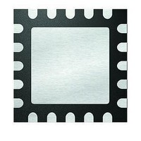
PIC18LF13K22-E/ML Microchip Technology, PIC18LF13K22-E/ML Datasheet - Page 109

PIC18LF13K22-E/ML
Manufacturer Part Number
PIC18LF13K22-E/ML
Description
8KB Flash, 256bytes RAM, 256bytes EEPROM, 16MIPS, NanoWatt XLP 20 QFN 4x4mm TUBE
Manufacturer
Microchip Technology
Series
PIC® XLP™ 18Fr
Datasheets
1.PIC18LF13K22-ISS.pdf
(388 pages)
2.PIC18LF13K22-ISS.pdf
(12 pages)
3.PIC18LF13K22-ISS.pdf
(36 pages)
Specifications of PIC18LF13K22-E/ML
Core Processor
PIC
Core Size
8-Bit
Speed
48MHz
Connectivity
I²C, LIN, SPI, UART/USART
Peripherals
Brown-out Detect/Reset, POR, PWM, WDT
Number Of I /o
17
Program Memory Size
8KB (4K x 16)
Program Memory Type
FLASH
Eeprom Size
256 x 8
Ram Size
256 x 8
Voltage - Supply (vcc/vdd)
1.8 V ~ 3.6 V
Data Converters
A/D 12x10b
Oscillator Type
Internal
Operating Temperature
-40°C ~ 125°C
Package / Case
20-VQFN Exposed Pad, 20-HVQFN, 20-SQFN, 20-DHVQFN
Processor Series
PIC18LF
Core
PIC
Data Bus Width
8 bit
Data Ram Size
256 B
Interface Type
EUSART, I2C, SPI
Maximum Clock Frequency
32 KHz
Number Of Programmable I/os
18
Number Of Timers
4
Operating Supply Voltage
1.8 V to 3.6 V
Maximum Operating Temperature
+ 125 C
Mounting Style
SMD/SMT
3rd Party Development Tools
52715-96, 52716-328, 52717-734, 52712-325, EWPIC18
Development Tools By Supplier
PG164130, DV164035, DV244005, DV164005
Minimum Operating Temperature
- 40 C
On-chip Adc
10 bit, 12 Channel
A/d Bit Size
10 bit
A/d Channels Available
12
Height
0.88 mm
Length
4 mm
Supply Voltage (max)
3.6 V
Supply Voltage (min)
1.8 V, 2.7 V
Width
4 mm
Lead Free Status / RoHS Status
Lead free / RoHS Compliant
Lead Free Status / RoHS Status
Lead free / RoHS Compliant
- Current page: 109 of 388
- Download datasheet (4Mb)
12.0
The Timer3 module timer/counter incorporates these
features:
• Software selectable operation as a 16-bit timer or
• Readable and writable 8-bit registers (TMR3H
• Selectable clock source (internal or external) with
• Interrupt-on-overflow
• Module Reset on CCP Special Event Trigger
REGISTER 12-1:
2010 Microchip Technology Inc.
bit 7
Legend:
R = Readable bit
-n = Value at POR
bit 7
bit 6
bit 5-4
bit 3
bit 2
bit 1
bit 0
counter
and TMR3L)
device clock or Timer1 oscillator internal options
R/W-0
RD16
TIMER3 MODULE
RD16: 16-bit Read/Write Mode Enable bit
1 = Enables register read/write of Timer3 in one 16-bit operation
0 = Enables register read/write of Timer3 in two 8-bit operations
Unimplemented: Read as ‘0’
T3CKPS<1:0>: Timer3 Input Clock Prescale Select bits
11 = 1:8 Prescale value
10 = 1:4 Prescale value
01 = 1:2 Prescale value
00 = 1:1 Prescale value
T3CCP1: Timer3 and Timer1 to CCP1 Enable bits
1 = Timer3 is the clock source for compare/capture of ECCP1
0 = Timer1 is the clock source for compare/capture of ECCP1
T3SYNC: Timer3 External Clock Input Synchronization Control bit
(Not usable if the device clock comes from Timer1/Timer3.)
When TMR3CS = 1:
1 = Do not synchronize external clock input
0 = Synchronize external clock input
When TMR3CS = 0:
This bit is ignored. Timer3 uses the internal clock when TMR3CS = 0.
TMR3CS: Timer3 Clock Source Select bit
1 = External clock input from Timer1 oscillator or T13CKI (on the rising edge after the first
0 = Internal clock (F
TMR3ON: Timer3 On bit
1 = Enables Timer3
0 = Stops Timer3
falling edge)
U-0
—
T3CON: TIMER3 CONTROL REGISTER
W = Writable bit
‘1’ = Bit is set
T3CKPS1
R/W-0
OSC
/4)
T3CKPS0
R/W-0
Preliminary
PIC18F1XK22/LF1XK22
U = Unimplemented bit, read as ‘0’
‘0’ = Bit is cleared
T3CCP1
R/W-0
A simplified block diagram of the Timer3 module is
shown in Figure 12-1. A block diagram of the module’s
operation in Read/Write mode is shown in Figure 12-2.
The Timer3 module is controlled through the T3CON
register (Register 12-1). It also selects the clock source
options for the CCP modules (see Section 13.1.1
“CCP Module and Timer Resources” for more
information).
T3SYNC
R/W-0
x = Bit is unknown
TMR3CS
R/W-0
DS41365D-page 109
TMR3ON
R/W-0
bit 0
Related parts for PIC18LF13K22-E/ML
Image
Part Number
Description
Manufacturer
Datasheet
Request
R

Part Number:
Description:
Manufacturer:
Microchip Technology Inc.
Datasheet:

Part Number:
Description:
Manufacturer:
Microchip Technology Inc.
Datasheet:

Part Number:
Description:
Manufacturer:
Microchip Technology Inc.
Datasheet:

Part Number:
Description:
Manufacturer:
Microchip Technology Inc.
Datasheet:

Part Number:
Description:
Manufacturer:
Microchip Technology Inc.
Datasheet:

Part Number:
Description:
Manufacturer:
Microchip Technology Inc.
Datasheet:

Part Number:
Description:
Manufacturer:
Microchip Technology Inc.
Datasheet:

Part Number:
Description:
Manufacturer:
Microchip Technology Inc.
Datasheet:


