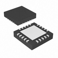
PIC18F14K22-E/ML Microchip Technology, PIC18F14K22-E/ML Datasheet - Page 241

PIC18F14K22-E/ML
Manufacturer Part Number
PIC18F14K22-E/ML
Description
16KB Flash, 512bytes RAM, 256bytes EEPROM, 16MIPS, 1.8-5.5V Operation 20 QFN 4x4
Manufacturer
Microchip Technology
Series
PIC® XLP™ 18Fr
Specifications of PIC18F14K22-E/ML
Core Processor
PIC
Core Size
8-Bit
Speed
48MHz
Connectivity
I²C, LIN, SPI, UART/USART
Peripherals
Brown-out Detect/Reset, POR, PWM, WDT
Number Of I /o
17
Program Memory Size
16KB (8K x 16)
Program Memory Type
FLASH
Eeprom Size
256 x 8
Ram Size
512 x 8
Voltage - Supply (vcc/vdd)
1.8 V ~ 5.5 V
Data Converters
A/D 12x10b
Oscillator Type
Internal
Operating Temperature
-40°C ~ 125°C
Package / Case
20-VQFN Exposed Pad, 20-HVQFN, 20-SQFN, 20-DHVQFN
Lead Free Status / RoHS Status
Lead free / RoHS Compliant
Available stocks
Company
Part Number
Manufacturer
Quantity
Price
Company:
Part Number:
PIC18F14K22-E/ML
Manufacturer:
MICROCHIP
Quantity:
1 000
- Current page: 241 of 388
- Download datasheet (4Mb)
REGISTER 19-2:
TABLE 19-2:
2010 Microchip Technology Inc.
bit 7
Legend:
R = Readable bit
-n = Value at POR
bit 7
bit 6
bit 5
bit 4
bit 3
bit 2
bit 1
bit 0
CM2CON1
INTCON3
SRCON0
SRCON1
TRISC
Legend: Shaded cells are not used with the SR Latch module.
SRSPE
Name
R/W-0
MC1OUT MC2OUT
TRISC7
SRSPE: SR Latch Peripheral Set Enable bit
1 = INT1 pin status sets SR latch
0 = INT1 pin status has no effect on SR latch
SRSCKE: SR Latch Set Clock Enable bit
1 = Set input of SR latch is pulsed with SRCLK
0 = Set input of SR latch is not pulsed with SRCLK
SRSC2E: SR Latch C2 Set Enable bit
1 = C2 Comparator output sets SR latch
0 = C2 Comparator output has no effect on SR latch
SRSC1E: SR Latch C1 Set Enable bit
1 = C1 Comparator output sets SR latch
0 = C1 Comparator output has no effect on SR latch
SRRPE: SR Latch Peripheral Reset Enable bit
1 = INT1 pin resets SR latch
0 = INT1 pin has no effect on SR latch
SRRCKE: SR Latch Reset Clock Enable bit
1 = Reset input of SR latch is pulsed with SRCLK
0 = Reset input of SR latch is not pulsed with SRCLK
SRRC2E: SR Latch C2 Reset Enable bit
1 = C2 Comparator output resets SR latch
0 = C2 Comparator output has no effect on SR latch
SRRC1E: SR Latch C1 Reset Enable bit
1 = C1 Comparator output resets SR latch
0 = C1 Comparator output has no effect on SR latch
SRLEN
SRSPE
INT2IP
Bit 7
REGISTERS ASSOCIATED WITH THE SR LATCH
SRSCKE
R/W-0
SRCON1: SR LATCH CONTROL REGISTER 1
SRSCKE
SRCLK2
TRISC6
INT1IP
Bit 6
W = Writable bit
‘1’ = Bit is set
SRSC2E
R/W-0
SRSC2E SRSC1E
C1RSEL
SRCLK1
TRISC5
Bit 5
—
SRSC1E
R/W-0
C2RSEL
SRCLK0
TRISC4
Preliminary
INT2IE
Bit 4
PIC18F1XK22/LF1XK22
U = Unimplemented
‘0’ = Bit is cleared
TRISC3
SRQEN
SRRPE
C1HYS
SRRPE
INT1IE
R/W-0
Bit 3
SRNQEN
SRRCKE
TRISC2
C2HYS
Bit 2
SRRCKE
—
R/W-0
C1SYNC
SRRC2E
TRISC1
INT2IF
SRPS
Bit 1
C = Clearable only bit
x = Bit is unknown
SRRC2E
R/W-0
C2SYNC
SRRC1E
TRISC0
INT1IF
SRPR
Bit 0
DS41365D-page 241
SRRC1E
R/W-0
on page
Values
Reset
260
257
260
260
260
bit 0
Related parts for PIC18F14K22-E/ML
Image
Part Number
Description
Manufacturer
Datasheet
Request
R

Part Number:
Description:
Manufacturer:
Microchip Technology Inc.
Datasheet:

Part Number:
Description:
Manufacturer:
Microchip Technology Inc.
Datasheet:

Part Number:
Description:
Manufacturer:
Microchip Technology Inc.
Datasheet:

Part Number:
Description:
Manufacturer:
Microchip Technology Inc.
Datasheet:

Part Number:
Description:
Manufacturer:
Microchip Technology Inc.
Datasheet:

Part Number:
Description:
Manufacturer:
Microchip Technology Inc.
Datasheet:

Part Number:
Description:
Manufacturer:
Microchip Technology Inc.
Datasheet:

Part Number:
Description:
Manufacturer:
Microchip Technology Inc.
Datasheet:


