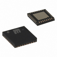
MICRF505YML TR Micrel Inc, MICRF505YML TR Datasheet - Page 21

MICRF505YML TR
Manufacturer Part Number
MICRF505YML TR
Description
868-915 MHz ISM Band Transceiver( )
Manufacturer
Micrel Inc
Specifications of MICRF505YML TR
Frequency
850MHz ~ 950MHz
Data Rate - Maximum
200kbps
Modulation Or Protocol
FSK
Applications
Telemetry, Wireless Controller
Power - Output
10dBm
Sensitivity
-111dBm
Voltage - Supply
2.3 V ~ 5.5 V
Current - Receiving
13.5mA
Current - Transmitting
28mA
Data Interface
PCB, Surface Mount
Antenna Connector
PCB, Surface Mount
Operating Temperature
-40°C ~ 85°C
Package / Case
32-MLF®, QFN
Operating Temperature (min)
-40C
Operating Temperature (max)
85C
Operating Temperature Classification
Industrial
Modulation Type
FSK
Lead Free Status / RoHS Status
Lead free / RoHS Compliant
Memory Size
-
Lead Free Status / Rohs Status
Compliant
Other names
576-1659-2
MICRF505YMLTR
MICRF505YMLTR
Switched Capacitor Filter
The main channel filter is a switched-capacitor
implementation of a six-pole elliptic low pass filter.
The elliptic filter minimized the total capacitance
required for a given selectivity and dynamic range.
The cut-off frequency of the switched-capacitor filter
is adjustable by changing the clock frequency.
The clock frequency is designed to be 20 times the
cut-off frequency. The clock frequency is derived
from
programmable 6-bit divider divides the frequency of
the crystal oscillator. To generate the correct non-
overlapping clock-phases needed by the filter this
frequency is then divided by 4. The cut-off frequency
of the filter is given by:
For instance, for a crystal frequency of 16MHz and if
the 6 bit divider divides the input frequency by 4 the
cut-off frequency of the SC filter is 16MHz/(40 x 4) =
100kHz. 1
to the output of the SC filter-to-filter the clock
frequency.
The lowest cutoff frequency in the pre- and the main
channel filter must be set so that the received signal
is passed with no attenuation, which is frequency
deviation plus modulation. If there are any frequency
offset between the transmitter and the receiver, this
must also be taken into consideration. A formula for
the receiver bandwidth can be summarized as
follows:
where
f
0001000
A6..A0
BW
October 2006
= + f
f
f
ScClk: Switched capacitor filter clock, bits
ScClk5-0
f
should not be smaller than f
f
receiver and transmitter [Hz]
f
chapter Modulator on how to calculate [Hz]
CUT
XCO
BW
OFFSET
DEV
D7
‘1’
the
: Needed receiver bandwidth, fcut above
OFFSET
: Filter cutoff frequency
: Single-sided frequency deviation, see
: Crystal oscillator frequency
st
order RC low pass filters are connected
:
D6
‘1’
reference
+ f
Total
f
CUT
ScClk5
DEV
D5
=
+ Baudrate / 2
frequency
ScClk4
40 ⋅ ScClk
D4
crystal
f
XCO
ScClk3
D3
BW
offset
ScClk2
[Hz]
D2
oscillator.
ScClk1
D1
between
ScClk0
D0
A
21
0000001
A6..A0
RSSI
A Typical plot of the RSSI voltage as function of
input power is shown in Figure 13. The RSSI has a
dynamic range of about 50dB from about -110dBm
to -60dBm input power.
The RSSI can be used as a signal presence
indicator. When a RF signal is received, the RSSI
output increases. This could be used to wake up
circuitry
configuration to conserve battery life.
Another application for which the RSSI could be
used is to determine if transmit power can be
reduced in a system. If the RSSI detects a strong
signal, if could tell the transmitter to reduce the
transmit power to reduce current consumption.
Modulation1
Baudrate: The baud rate given is bit/sec
Pin 14
RSSI
D7
2.2
1.8
1.6
1.4
1.2
0.8
0.6
2
1
-125
that
-115
Modulation0
Figure 14. RSSI Network
Figure 13. RSSI Voltage
is
D6
-105
33kohm, 1nF, 125kbps, BW=200kHz, Vdd=2.5V
-95
normally
R2
33k
D5
‘0’
-85
RSSI
Pin [dBm]
D4
‘0’
-75
-65
RSSI_en
in
D3
-55
C10
1nF
a
+1 408-944-0800
-45
LD_en
M9999-103106
D2
sleep
-35
RSSI
PF_FC1
-25
D1
mode
PF_FC0
D0


