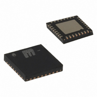
MICRF505YML TR Micrel Inc, MICRF505YML TR Datasheet - Page 18

MICRF505YML TR
Manufacturer Part Number
MICRF505YML TR
Description
868-915 MHz ISM Band Transceiver( )
Manufacturer
Micrel Inc
Specifications of MICRF505YML TR
Frequency
850MHz ~ 950MHz
Data Rate - Maximum
200kbps
Modulation Or Protocol
FSK
Applications
Telemetry, Wireless Controller
Power - Output
10dBm
Sensitivity
-111dBm
Voltage - Supply
2.3 V ~ 5.5 V
Current - Receiving
13.5mA
Current - Transmitting
28mA
Data Interface
PCB, Surface Mount
Antenna Connector
PCB, Surface Mount
Operating Temperature
-40°C ~ 85°C
Package / Case
32-MLF®, QFN
Operating Temperature (min)
-40C
Operating Temperature (max)
85C
Operating Temperature Classification
Industrial
Modulation Type
FSK
Lead Free Status / RoHS Status
Lead free / RoHS Compliant
Memory Size
-
Lead Free Status / Rohs Status
Compliant
Other names
576-1659-2
MICRF505YMLTR
MICRF505YMLTR
Charge Pump
The charge pump current can be set to either 125µA
or 500µA by CP_HI (‘1’ → 500µA). This will affect
the loop filter component values, see “PLL Filter”
section. In most cases, the low current is best suited.
For applications using phase detector frequency and
high PLL bandwidth, the 500µA can be a better
choice.
PLL Filter
The design of the PLL filter will strongly affect the
performance of the frequency synthesizer. The PLL
filter is kept externally for flexibility. Input parameters
when designing the loop filter for the MICRF505 are
mainly the modulation method and the bit rate.
These choices will also affect the switching time and
phase noise.
The frequency modulation can be done in two
different ways with the MICRF505, either by VCO
modulation or by modulation with the internal
dividers (see chapter Frequency modulation for
further details). In the first case, the PLL needs to
lock on a new carrier frequency for every new data
bit. Now the PLL bandwidth needs to be adequately
high. It is recommended to use a third order filter to
suppress the phase detector frequency, as this is
not suppressed as much as when doing modulation
on the VCO with a lower bandwidth filter.
A schematic for a second (R2=0 and C3=NC) and
third order loop filter is shown in Figure 8.
October 2006
0000010
A6..A0
Figure 8. Second and Third Order Loop Filter
CP_OUT
Pin 27
CP_HI
D7
SC_by
D6
D5
‘0’
C1
PA_by
D4
R1
C2
OUTS3
R2
D3
OUTS2
D2
C3
OUTS1
D1
VARIN
Pin 29
OUTS1
D0
18
Divider
0000000
0000001
VCO
VCO
A6..A0
A6..A0
Table 9 shows three different loop filters, the two first
for VCO modulation and the last one for modulation
using the internal dividers. The component values
are calculated with RF frequency = 915MHz, VCO
gain = 67MHz/V and charge pump current = 125µA.
Other settings are shown in the table. The varactor
pin capacitance (pin 29) of 5pF does not influence
on the component values for the two filters with
lowest bandwidth.
Lock Detect
Modes of Operation
Mode1
A lock detector can be enabled by setting LD_en
= 1. When pin LD is high, it indicates that the
PLL is in lock.
0
0
1
1
(kbaud/sec)
Baud Rate
Modulation1
LNA_by
>38.4
>125
Table 9. Loop Filter Components Values
<20
D7
D7
Mode0
0
1
0
1
(kHz)
PA2
PLL
D6
BW
0.8
3.2
Modulation0
13
D6
Power down
Margin(˚)
PA1
D5
Transmit
Phase
Standby
Receive
State
56
56
86
D5
‘0’
PA0
D4
Detector
Phase
Freq.
(kHz)
D4
100
100
500
‘0’
Sync_en
Comments
Keeps register configuration
Only crystal oscillator running
Full receive
Full transmit ex PA state
D3
RSSI_en
680pF
150pF
D3
10nF
C1
Mode1
+1 408-944-0800
100nF 6.2kΩ
6.8nF
D2
10nF
LD_en
M9999-103106
C2
D2
22kΩ
18kΩ
Mode0
R1
PF_FC1
D1
D1
82kΩ
R2
0
0
Load_en
PF_FC0
D0
D0
4.7pF
NC
NC
C3


