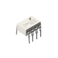
ML2035CP Fairchild Semiconductor, ML2035CP Datasheet - Page 7

ML2035CP
Manufacturer Part Number
ML2035CP
Description
RF Receiver DIP-8 SINE WAVE GEN
Manufacturer
Fairchild Semiconductor
Type
Infrared Remote Control Receiverr
Datasheet
1.ML2035CP.pdf
(9 pages)
Specifications of ML2035CP
Package / Case
DIP-8
Operating Supply Voltage
6.3 V
Maximum Operating Temperature
80 C
Minimum Operating Temperature
- 30 C
Mounting Style
Through Hole
Lead Free Status / RoHS Status
Lead free / RoHS Compliant
Available stocks
Company
Part Number
Manufacturer
Quantity
Price
Company:
Part Number:
ML2035CP
Manufacturer:
FSC
Quantity:
1 156
Company:
Part Number:
ML2035CP
Manufacturer:
MIC
Quantity:
6 250
FUNCTIONAL DESCRIPTION
SERIAL DIGITAL INTERFACE
The digital interface consists of a shift register and data
latch. The serial 16-bit data word on SID is clocked into a
16-bit shift register on rising edges of the serial shift clock,
SCK. The LSB should be shifted in first and the MSB last as
shown in Figure 4. The data that has been shifted into the
shift register is loaded into a 16-bit data latch on the
falling edge of LATI. To insure that true data is loaded into
the data latch from the shift register, LATI falling edge
should occur when SCK is low, as shown in figure 1. LATI
should be low while shifting data into the shift register to
avoid inadvertently entering the power down mode. Note
that all data is entered and latched on the edges, not
levels, of SCK and LATI.
POWER DOWN MODE
The power down mode of the ML2035 can be selected by
entering all zeros in the shift register and applying a logic
“1” to LATI and holding it high. A zero data detect circuit
detects when all bits in the shift register are zeros. In this
state, the power consumption is reduced to 11.5mW max,
and V
10k to ground. The master clock, CLK IN, can be left
active or removed during power down mode.
REV. 1.0 10/10/2000
LATI
SCK
SID
OUT
goes to 0V as shown in Figure 5 and appears as
0
POWER DOWN MODE
1
2
3
Figure 5. Power Down Mode Waveforms.
4
(Continued)
LATI
SCK
Figure 4. Serial Interface Timing.
SID
0V
5
V
OS
6
7
0 1 2 3 4 5 6 7 8 9 10 11 12 131415
8
POWER SUPPLIES
The analog circuits in ML2035 are powered from V
V
device are powered from V
It is recommended that the power supplies to the device
should be bypassed by placing decoupling capacitors
from V
the device as possible.
9
SS
and are referenced to GND. The digital circuits in the
10
CC
11
to GND and V
12
13
14
SS
to GND as physically close to
CC
15
to GND.
ML2035
CC
to
7


