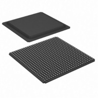
XC3SD1800A-4FG676I Xilinx Inc, XC3SD1800A-4FG676I Datasheet - Page 43

XC3SD1800A-4FG676I
Manufacturer Part Number
XC3SD1800A-4FG676I
Description
FPGA Spartan®-3A Family 1.8M Gates 37440 Cells 667MHz 90nm Technology 1.2V 676-Pin FBGA
Manufacturer
Xilinx Inc
Series
Spartan™-3A DSPr
Datasheets
1.XC3S50A-4VQG100C.pdf
(7 pages)
2.XC3SD3400A-4FGG676C.pdf
(4 pages)
3.XC3SD3400A-4FGG676C.pdf
(101 pages)
Specifications of XC3SD1800A-4FG676I
Package
676FBGA
Family Name
Spartan®-3A
Device Logic Units
37440
Device System Gates
1800000
Maximum Internal Frequency
667 MHz
Typical Operating Supply Voltage
1.2 V
Maximum Number Of User I/os
519
Ram Bits
1548288
Number Of Logic Elements/cells
37440
Number Of Labs/clbs
4160
Total Ram Bits
1548288
Number Of I /o
519
Number Of Gates
1800000
Voltage - Supply
1.14 V ~ 1.26 V
Mounting Type
Surface Mount
Operating Temperature
-40°C ~ 100°C
Package / Case
676-BBGA
Lead Free Status / RoHS Status
Contains lead / RoHS non-compliant
For Use With
122-1574 - KIT DEVELOPMENT SPARTAN 3ADSP
Lead Free Status / RoHS Status
Contains lead / RoHS non-compliant
Available stocks
Company
Part Number
Manufacturer
Quantity
Price
Company:
Part Number:
XC3SD1800A-4FG676I
Manufacturer:
XilinxInc
Quantity:
3 000
Company:
Part Number:
XC3SD1800A-4FG676I
Manufacturer:
Xilinx Inc
Quantity:
10 000
Part Number:
XC3SD1800A-4FG676I
Manufacturer:
XILINX/赛灵思
Quantity:
20 000
Table 35: Clock to Out, Propagation Delays, and Maximum Frequency for the DSP48A
DS610 (v3.0) October 4, 2010
Product Specification
Notes:
1.
2.
3.
Clock to Out from Output Register Clock to Output Pin
T
Clock to Out from Pipeline Register Clock to Output Pins
T
Clock to Out from Input Register Clock to Output Pins
T
T
T
T
Combinatorial Delays from Input Pins to Output Pins
T
T
T
T
T
T
Maximum Frequency
F
DSPCKO_PP
DSPCKO_PM
DSPCKO_PA
DSPCKO_PB
DSPCKO_PC
DSPCKO_PD
DSPDO_AP
DSPDO_BP
DSPDO_BP
DSPDO_CP
DSPDO_DP
DSPDO_OPP
MAX
Symbol
To reference the DSP48A block diagram, see UG431: XtremeDSP DSP48A for Spartan-3A DSP FPGA User Guide.
"Yes" means that the component is in the path. "No" means that the component is being bypassed. “–“ means that no path exists, so it is not
applicable.
The numbers in this table are based on the operating conditions set forth in
CLK (PREG) to P output
CLK (MREG) to P output
CLK (AREG) to P output
CLK (BREG) to P output
CLK (CREG) to P output
CLK (DREG) to P output
A or B input to P output
B input to P output
C input to P output
D input to P output
OPMODE input to P output
All registers used
Description
Spartan-3A DSP FPGA Family: DC and Switching Characteristics
www.xilinx.com
Pre-adder
Yes
Yes
Yes
Yes
Yes
Yes
Yes
Yes
–
–
–
–
–
–
–
–
–
Multiplier Post-adder
Table
Yes
Yes
Yes
Yes
Yes
Yes
Yes
Yes
Yes
Yes
Yes
Yes
No
No
–
–
–
7.
Yes
Yes
Yes
Yes
Yes
Yes
Yes
Yes
Yes
Yes
Yes
Yes
No
No
No
No
–
Max
1.26
3.16
1.94
6.33
7.45
3.37
7.33
2.78
4.60
5.65
3.49
5.79
6.74
2.76
6.81
7.12
287
Speed Grade
-5
Max
1.44
3.63
2.23
7.27
8.56
3.87
8.42
3.19
5.28
6.49
4.01
6.65
7.74
3.17
7.82
8.18
250
-4
Units
MHz
ns
ns
ns
ns
ns
ns
ns
ns
ns
ns
ns
ns
ns
ns
ns
ns
43


