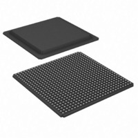
XC3SD1800A-4FG676I Xilinx Inc, XC3SD1800A-4FG676I Datasheet - Page 33

XC3SD1800A-4FG676I
Manufacturer Part Number
XC3SD1800A-4FG676I
Description
FPGA Spartan®-3A Family 1.8M Gates 37440 Cells 667MHz 90nm Technology 1.2V 676-Pin FBGA
Manufacturer
Xilinx Inc
Series
Spartan™-3A DSPr
Datasheets
1.XC3S50A-4VQG100C.pdf
(7 pages)
2.XC3SD3400A-4FGG676C.pdf
(4 pages)
3.XC3SD3400A-4FGG676C.pdf
(101 pages)
Specifications of XC3SD1800A-4FG676I
Package
676FBGA
Family Name
Spartan®-3A
Device Logic Units
37440
Device System Gates
1800000
Maximum Internal Frequency
667 MHz
Typical Operating Supply Voltage
1.2 V
Maximum Number Of User I/os
519
Ram Bits
1548288
Number Of Logic Elements/cells
37440
Number Of Labs/clbs
4160
Total Ram Bits
1548288
Number Of I /o
519
Number Of Gates
1800000
Voltage - Supply
1.14 V ~ 1.26 V
Mounting Type
Surface Mount
Operating Temperature
-40°C ~ 100°C
Package / Case
676-BBGA
Lead Free Status / RoHS Status
Contains lead / RoHS non-compliant
For Use With
122-1574 - KIT DEVELOPMENT SPARTAN 3ADSP
Lead Free Status / RoHS Status
Contains lead / RoHS non-compliant
Available stocks
Company
Part Number
Manufacturer
Quantity
Price
Company:
Part Number:
XC3SD1800A-4FG676I
Manufacturer:
XilinxInc
Quantity:
3 000
Company:
Part Number:
XC3SD1800A-4FG676I
Manufacturer:
Xilinx Inc
Quantity:
10 000
Part Number:
XC3SD1800A-4FG676I
Manufacturer:
XILINX/赛灵思
Quantity:
20 000
Table 26: Test Methods for Timing Measurement at I/Os (Cont’d)
The capacitive load (C
speed files and the data sheet, is always based on a C
all measurements. Any delay that the test fixture might contribute to test measurements is subtracted from those
measurements to produce the final timing numbers as published in the speed files and data sheet.
DS610 (v3.0) October 4, 2010
Product Specification
Notes:
1.
2.
3.
Differential
LVDS_25
LVDS_33
BLVDS_25
MINI_LVDS_25
MINI_LVDS_33
LVPECL_25
LVPECL_33
RSDS_25
RSDS_33
TMDS_33
PPDS_25
PPDS_33
DIFF_HSTL_I_18
DIFF_HSTL_II_18
DIFF_HSTL_III_18
DIFF_HSTL_I
DIFF_HSTL_III
DIFF_SSTL18_I
DIFF_SSTL18_II
DIFF_SSTL2_I
DIFF_SSTL2_II
DIFF_SSTL3_I
DIFF_SSTL3_II
Descriptions of the relevant symbols are:
V
V
V
V
V
R
V
The load capacitance (C
According to the PCI specification. For information on PCI IP solutions, see www.xilinx.com/pci. The PCIX IOSTANDARD is available and
has equivalent characteristics but no PCI-X IP is supported.
REF
ICM
M
L
H
T
Signal Standard
T
(IOSTANDARD)
– Low-level test voltage at Input pin
– Effective termination resistance, which takes on a value of 1 MΩ when no parallel termination is required
– Termination voltage
– High-level test voltage at Input pin
– Voltage of measurement point on signal transition
– The common mode input voltage
– The reference voltage for setting the input switching threshold
L
) is connected between the output and GND. The Output timing for all standards, as published in the
L
) at the Output pin is 0 pF for all signal standards.
V
REF
–
–
–
–
–
–
–
–
–
–
–
–
–
–
–
–
–
–
–
–
–
–
–
(V)
V
V
V
V
V
V
V
V
V
V
V
V
V
V
V
V
V
V
V
V
V
V
V
ICM
ICM
ICM
ICM
ICM
ICM
ICM
ICM
ICM
ICM
ICM
ICM
ICM
ICM
ICM
ICM
ICM
ICM
ICM
ICM
ICM
ICM
ICM
V
Inputs
L
– 0.125
– 0.125
– 0.125
– 0.125
– 0.125
(V)
– 0.3
– 0.3
– 0.1
– 0.1
– 0.1
– 0.1
– 0.1
– 0.5
– 0.5
– 0.5
– 0.5
– 0.5
– 0.5
– 0.5
– 0.5
– 0.5
– 0.5
– 0.5
Spartan-3A DSP FPGA Family: DC and Switching Characteristics
L
www.xilinx.com
value of zero. High-impedance probes (less than 1 pF) are used for
V
V
V
V
V
V
V
V
V
V
V
V
V
V
V
V
V
V
V
V
V
V
V
ICM
ICM
ICM
ICM
ICM
ICM
ICM
ICM
ICM
ICM
ICM
ICM
ICM
ICM
ICM
ICM
ICM
ICM
ICM
ICM
ICM
ICM
ICM
V
H
+ 0.125
+ 0.125
+ 0.125
+ 0.125
+ 0.125
(V)
+ 0.3
+ 0.3
+ 0.1
+ 0.1
+ 0.1
+ 0.1
+ 0.1
+ 0.5
+ 0.5
+ 0.5
+ 0.5
+ 0.5
+ 0.5
+ 0.5
+ 0.5
+ 0.5
+ 0.5
+ 0.5
R
N/A
N/A
T
1M
50
50
50
50
50
50
50
50
50
50
50
50
50
50
50
50
50
50
50
50
(Ω)
Outputs
(2)
V
1.25
1.25
N/A
N/A
T
1.2
1.2
1.2
1.2
1.2
1.2
3.3
0.8
0.8
0.9
0.9
1.8
0.9
0.9
0.9
0.9
1.5
1.5
0
(V)
Inputs and
Outputs
V
V
V
V
V
V
V
V
V
V
V
V
V
V
V
V
V
V
V
V
V
V
V
V
M
ICM
ICM
ICM
ICM
ICM
ICM
ICM
ICM
ICM
ICM
ICM
ICM
ICM
ICM
ICM
ICM
ICM
ICM
ICM
ICM
ICM
ICM
ICM
(V)
33


