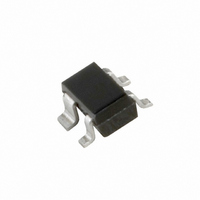
BFG310W/XR,115 NXP Semiconductors, BFG310W/XR,115 Datasheet - Page 3

BFG310W/XR,115
Manufacturer Part Number
BFG310W/XR,115
Description
TRANS NPN 6V 10MA 14GHZ SOT343R
Manufacturer
NXP Semiconductors
Datasheet
1.BFG310WXR115.pdf
(12 pages)
Specifications of BFG310W/XR,115
Package / Case
CMPAK-4
Transistor Type
NPN
Voltage - Collector Emitter Breakdown (max)
6V
Frequency - Transition
14GHz
Noise Figure (db Typ @ F)
1dB @ 2GHz
Gain
18dB
Power - Max
60mW
Dc Current Gain (hfe) (min) @ Ic, Vce
60 @ 5mA, 3V
Current - Collector (ic) (max)
10mA
Mounting Type
Surface Mount
Dc Collector/base Gain Hfe Min
60
Dc Current Gain Hfe Max
60 @ 5mA @ 3V
Mounting Style
SMD/SMT
Configuration
Single
Transistor Polarity
NPN
Maximum Operating Frequency
14 GHz
Collector- Emitter Voltage Vceo Max
6 V
Emitter- Base Voltage Vebo
2 V
Continuous Collector Current
10 mA
Power Dissipation
60 mW
Maximum Operating Temperature
+ 175 C
Lead Free Status / RoHS Status
Lead free / RoHS Compliant
Lead Free Status / RoHS Status
Lead free / RoHS Compliant, Lead free / RoHS Compliant
Other names
568-1976-2
934057941115
BFG310W/XR T/R
934057941115
BFG310W/XR T/R
Available stocks
Company
Part Number
Manufacturer
Quantity
Price
Part Number:
BFG310W/XR,115
Manufacturer:
NXP/恩智浦
Quantity:
20 000
Philips Semiconductors
5. Limiting values
Table 5:
In accordance with the Absolute Maximum Rating System (IEC 60134).
[1]
6. Thermal characteristics
Table 6:
[1]
7. Characteristics
Table 7:
T
9397 750 14245
Product data sheet
Symbol
V
V
V
I
P
T
T
Symbol Parameter
R
Symbol Parameter
I
h
C
C
C
f
MSG
NF
P
IP3
s
C
CBO
T
j
FE
stg
j
CBO
CEO
EBO
tot
L(1dB)
th(j-sp)
CBS
CES
EBS
21
= 25 C; unless otherwise specified.
2
T
T
sp
sp
is the temperature at the soldering point of the collector pin.
is the temperature at the soldering point of the collector pin.
thermal resistance from junction to solder point
collector-base cut-off current
DC current gain
collector-base capacitance
collector-emitter capacitance
emitter-base capacitance
transition frequency
maximum stable gain
insertion power gain
noise figure
output power at 1 dB gain
compression
third order intercept point
Limiting values
Thermal characteristics
Characteristics
Parameter
collector-base voltage
collector-emitter voltage
emitter-base voltage
collector current (DC)
total power dissipation
storage temperature
junction temperature
Conditions
I
I
V
V
V
I
T
I
T
I
Z
I
T
I
T
E
C
C
C
C
C
C
amb
amb
S
s
amb
amb
CB
CE
EB
f = 1.8 GHz
f = 3 GHz
= 0 A; V
= 5 mA; V
= 5 mA; V
= 5 mA; V
= 5 mA; V
= 5 mA; V
= 5 mA; V
=
= Z
= 5 V; f = 1 MHz; emitter grounded
= 5 V; f = 1 MHz; base grounded
= 0.5 V; f = 1 MHz; collector grounded
Rev. 01 — 2 February 2005
= 25 C
= 25 C
= 25 C; Z
= 25 C; Z
opt
L
= 50
; I
C
CB
Conditions
open emitter
open base
open collector
T
= 1 mA; V
CE
CE
CE
CE
CE
CE
sp
= 6 V
= 3 V
= 3 V; f = 1 GHz;
= 3 V; f = 1.8 GHz;
= 3 V; T
= 3 V; f = 1.8 GHz;
= 3 V; f = 1.8 GHz;
S
S
145 C
= Z
= Z
L
L
CE
= 50
= 50
Conditions
T
amb
sp
= 3 V; f = 2 GHz
= 25 C;
145 C
NPN 14 GHz wideband transistor
© Koninklijke Philips Electronics N.V. 2005. All rights reserved.
[1]
BFG310W/XR
Min
-
60
-
-
-
-
-
-
-
-
-
-
Min
-
-
-
-
-
-
65
Typ
-
100
0.17
0.22
0.16
14
18
14
11
1
1.8
8.5
[1]
Max
15
6
2
10
60
+175
175
Typ
530
Max
15
200
0.3
-
-
-
-
-
-
-
-
-
Unit
V
V
V
mA
mW
C
C
Unit
K/W
3 of 12
Unit
nA
pF
pF
pF
GHz
dB
dB
dB
dB
dBm
dBm


