PSMN005-25D,118 NXP Semiconductors, PSMN005-25D,118 Datasheet - Page 2
PSMN005-25D,118
Manufacturer Part Number
PSMN005-25D,118
Description
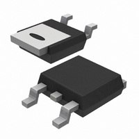
MOSFET N-CH 25V 75A SOT428
Manufacturer
NXP Semiconductors
Series
TrenchMOS™r
Datasheet
1.PSMN005-25D118.pdf
(12 pages)
Specifications of PSMN005-25D,118
Fet Type
MOSFET N-Channel, Metal Oxide
Fet Feature
Logic Level Gate
Rds On (max) @ Id, Vgs
5.8 mOhm @ 25A, 10V
Drain To Source Voltage (vdss)
25V
Current - Continuous Drain (id) @ 25° C
75A
Vgs(th) (max) @ Id
2V @ 1mA
Gate Charge (qg) @ Vgs
60nC @ 5V
Input Capacitance (ciss) @ Vds
3500pF @ 20V
Power - Max
125W
Mounting Type
Surface Mount
Package / Case
DPak, TO-252 (2 leads+tab), SC-63
Configuration
Single Dual Drain
Transistor Polarity
N-Channel
Resistance Drain-source Rds (on)
0.0058 Ohms
Drain-source Breakdown Voltage
25 V
Gate-source Breakdown Voltage
+/- 15 V
Continuous Drain Current
75 A
Power Dissipation
125 W
Maximum Operating Temperature
+ 175 C
Mounting Style
SMD/SMT
Minimum Operating Temperature
- 55 C
Lead Free Status / RoHS Status
Lead free / RoHS Compliant
Other names
934055816118
PSMN005-25D /T3
PSMN005-25D /T3
PSMN005-25D /T3
PSMN005-25D /T3


Philips Semiconductors
October 1999
FEATURES
• ’Trench’ technology
• Very low on-state resistance
• Fast switching
• Logic level compatible
SiliconMAX products use the latest
Philips
achieve
on-state
package at each voltage rating.
Applications:-
• d.c. to d.c. converters
• switched mode power supplies
The PSMN005-25D is supplied in
the
mounting package.
LIMITING VALUES
Limiting values in accordance with the Absolute Maximum System (IEC 134)
1 It is not possible to make connection to pin 2 of the SOT428 package.
2 Continuous current rating limited by package.
GENERAL DESCRIPTION
SYMBOL PARAMETER
V
V
V
V
I
I
P
T
N-channel logic level TrenchMOS
D
DM
j
DSS
DGR
GS
GSM
D
, T
stg
SOT428
Trench
the
resistance
Drain-source voltage
Drain-gate voltage
Continuous gate-source
voltage
Peak pulsed gate-source
voltage
Continuous drain current
Pulsed drain current
Total power dissipation
Operating junction and
storage temperature
lowest
(Dpak)
technology
in
possible
surface
each
to
PINNING
SYMBOL
PIN
tab
1
2
3
CONDITIONS
T
T
T
T
T
T
T
j
j
j
mb
mb
mb
mb
= 25 ˚C to 175˚C
= 25 ˚C to 175˚C; R
= 25 ˚C; V
= 100 ˚C; V
= 25 ˚C
= 25 ˚C
150 ˚C
gate
drain
source
drain
g
1
DESCRIPTION
(TM)
2
GS
GS
d
s
= 5 V
transistor
= 5 V
GS
= 20 k
QUICK REFERENCE DATA
R
SOT428 (DPAK)
R
DS(ON)
DS(ON)
MIN.
- 55
V
5.8 m (V
-
-
-
-
-
-
-
-
7.5 m (V
PSMN005-25D
I
DSS
D
Product specification
1
= 75 A
= 25 V
tab
2
MAX.
240
125
175
75
25
25
70
3
15
20
2
GS
GS
= 10 V)
Rev 1.100
= 5 V)
UNIT
˚C
W
V
V
V
V
A
A
A
Related parts for PSMN005-25D,118
Image
Part Number
Description
Manufacturer
Datasheet
Request
R

Part Number:
Description:
MOSFET N-CH 75V 75A D2PAK
Manufacturer:
NXP Semiconductors
Datasheet:
Part Number:
Description:
MOSFET N-CH 55V 75A SOT404
Manufacturer:
NXP Semiconductors
Datasheet:

Part Number:
Description:
SiliconMAX standard level N-channel enhancement mode Field-Effect Transistor (FET) in a plastic package using TrenchMOS technology
Manufacturer:
NXP Semiconductors
Datasheet:

Part Number:
Description:
MOSFET N-CH 30V 20A SOT96-1
Manufacturer:
NXP Semiconductors
Datasheet:

Part Number:
Description:
SiliconMAX logic level N-channel enhancement mode Field-Effect Transistor (FET) in a plastic package using TrenchMOS technology
Manufacturer:
NXP Semiconductors
Datasheet:

Part Number:
Description:
N-channel Logic Level Field-effect Power Transistor In A Plastic Package Using Trenchmos Technology.
Manufacturer:
NXP Semiconductors
Datasheet:
Part Number:
Description:
Psmn005-25d N-channel Logic Level Trenchmos Tm Transistor
Manufacturer:
NXP Semiconductors
Datasheet:
Part Number:
Description:
Psmn005-30k Trenchmos Tm Logic Level Fet
Manufacturer:
NXP Semiconductors
Datasheet:

Part Number:
Description:
MOSFET N-CH 55V 75A SOT78
Manufacturer:
NXP Semiconductors
Datasheet:
Part Number:
Description:
MOSFET N-CH 75V 75A TO220AB
Manufacturer:
NXP Semiconductors
Datasheet:
Part Number:
Description:
MOSFET TAPE13 PWR-MOS
Manufacturer:
NXP Semiconductors
Datasheet:

Part Number:
Description:
N-channel logic level TrenchMOS transistor
Manufacturer:
PHILIPS [NXP Semiconductors]
Datasheet:
Part Number:
Description:
NXP Semiconductors designed the LPC2420/2460 microcontroller around a 16-bit/32-bitARM7TDMI-S CPU core with real-time debug interfaces that include both JTAG andembedded trace
Manufacturer:
NXP Semiconductors
Datasheet: