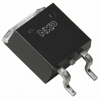
BUK9624-55A,118 NXP Semiconductors, BUK9624-55A,118 Datasheet - Page 2

BUK9624-55A,118
Manufacturer Part Number
BUK9624-55A,118
Description
MOSFET N-CH 55V 46A D2PAK
Manufacturer
NXP Semiconductors
Series
TrenchMOS™r
Specifications of BUK9624-55A,118
Package / Case
D²Pak, TO-263 (2 leads + tab)
Fet Type
MOSFET N-Channel, Metal Oxide
Fet Feature
Logic Level Gate
Rds On (max) @ Id, Vgs
21.7 mOhm @ 25A, 10V
Drain To Source Voltage (vdss)
55V
Current - Continuous Drain (id) @ 25° C
46A
Vgs(th) (max) @ Id
2V @ 1mA
Input Capacitance (ciss) @ Vds
1815pF @ 25V
Power - Max
105W
Mounting Type
Surface Mount
Minimum Operating Temperature
- 55 C
Configuration
Single
Transistor Polarity
N-Channel
Resistance Drain-source Rds (on)
0.0217 Ohm @ 10 V
Drain-source Breakdown Voltage
55 V
Gate-source Breakdown Voltage
+/- 10 V
Continuous Drain Current
46 A
Power Dissipation
105000 mW
Maximum Operating Temperature
+ 175 C
Mounting Style
SMD/SMT
Lead Free Status / RoHS Status
Lead free / RoHS Compliant
Gate Charge (qg) @ Vgs
-
Lead Free Status / Rohs Status
Lead free / RoHS Compliant
Other names
934056287118
BUK9624-55A /T3
BUK9624-55A /T3
BUK9624-55A /T3
BUK9624-55A /T3
5. Quick reference data
Table 2:
6. Limiting values
Table 3:
In accordance with the Absolute Maximum Rating System (IEC 60134).
Philips Semiconductors
9397 750 07538
Product specification
Symbol Parameter
V
I
P
T
R
Symbol Parameter
V
V
V
V
I
I
P
T
T
Source-drain diode
I
I
Avalanche ruggedness
W
D
D
DM
DR
DRM
j
stg
j
DS
tot
DS
DGR
GS
GSM
tot
DSon
DSS
drain-source voltage (DC)
drain current (DC)
total power dissipation
junction temperature
drain-source on-state resistance
drain-source voltage (DC)
drain-gate voltage (DC)
gate-source voltage (DC)
non-repetitive gate-source voltage
drain current (DC)
peak drain current
total power dissipation
storage temperature
operating junction temperature
reverse drain current (DC)
pulsed reverse drain current
non-repetitive avalanche energy
Quick reference data
Limiting values
Rev. 01 — 29 September 2000
Conditions
T
T
V
V
Conditions
t
T
Figure 2
T
T
Figure 3
T
T
T
unclamped inductive load; I
V
starting T
R
p
mb
mb
mb
mb
mb
mb
mb
mb
GS
GS
DS
GS
50 s
= 25 C; V
= 25 C
= 25 C; V
= 100 C; V
= 25 C; pulsed; t
= 25 C;
= 25 C
= 25 C; pulsed; t
= 5 V; I
= 4.5 V; I
BUK9524-55A; BUK9624-55A
= 20 k
25 V; V
and
mb
D
= 25 C
3
Figure 1
= 25 A
D
GS
GS
GS
= 25 A
GS
= 5 V; R
= 5 V
= 5 V;
= 5 V;
p
p
GS
10 s
10 s;
Figure 2
D
= 50 ;
= 46 A;
TrenchMOS™ logic level FET
Typ
20
Min
55
55
© Philips Electronics N.V. 2000. All rights reserved.
Max
55
46
105
175
24
26
Max
55
55
46
33
188
105
+175
+175
46
188
76
10
15
Unit
V
A
W
m
m
Unit
V
V
V
V
A
A
A
W
A
A
mJ
C
C
C
2 of 15


