FCB11N60TM Fairchild Semiconductor, FCB11N60TM Datasheet
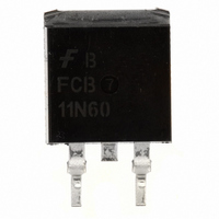
MOSFET N-CH 600V 11A D2PAK

FCB11N60TM

Manufacturer Part Number
FCB11N60TM
Description
MOSFET N-CH 600V 11A D2PAK
Manufacturer
Fairchild Semiconductor
Series
SuperFET™r
Type
Power MOSFETr
Datasheet

Specifications of FCB11N60TM

Fet Type
MOSFET N-Channel, Metal Oxide
Fet Feature
Standard
Rds On (max) @ Id, Vgs
380 mOhm @ 5.5A, 10V
Drain To Source Voltage (vdss)
600V
Current - Continuous Drain (id) @ 25° C
11A
Vgs(th) (max) @ Id
5V @ 250µA
Gate Charge (qg) @ Vgs
52nC @ 10V
Input Capacitance (ciss) @ Vds
1490pF @ 25V
Power - Max
125W
Mounting Type
Surface Mount
Package / Case
D²Pak, TO-263 (2 leads + tab)
Configuration
Single
Transistor Polarity
N-Channel
Resistance Drain-source Rds (on)
0.38 Ohms
Drain-source Breakdown Voltage
600 V
Gate-source Breakdown Voltage
+/- 30 V
Continuous Drain Current
11 A
Power Dissipation
125 W
Maximum Operating Temperature
+ 150 C
Mounting Style
SMD/SMT
Minimum Operating Temperature
- 55 C
Number Of Elements
1
Polarity
N
Channel Mode
Enhancement
Drain-source On-res
0.38Ohm
Drain-source On-volt
600V
Gate-source Voltage (max)
±30V
Operating Temp Range
-55C to 150C
Operating Temperature Classification
Military
Mounting
Surface Mount
Pin Count
2 +Tab
Package Type
D2PAK
Lead Free Status / RoHS Status
Lead free / RoHS Compliant
Other names
FCB11N60TMTR
FCB11N60TM_NL
FCB11N60TM_NLTR
FCB11N60TM_NLTR

Available stocks

Company
Part Number
Manufacturer
Quantity
Price
Company:
Part Number:
FCB11N60TM
Quantity:
3 375
©2005 Fairchild Semiconductor Corporation
FCB11N60 Rev. A1
FCB11N60
600V N-Channel MOSFET
Features
• 650V @T
• Typ. R
• Ultra low gate charge (typ. Q
• Low effective output capacitance (typ. C
• 100% avalanche tested
Absolute Maximum Ratings
Thermal Characteristics
* When mounted on the minimum pad size recommended (PCB Mount)
V
I
I
V
E
I
E
dv/dt
P
T
T
R
R
R
D
DM
AR
J,
L
DSS
GSS
AS
AR
D
Symbol
Symbol
θJC
θJA
θJA
T
STG
*
DS(on)
J
= 150°C
= 0.32Ω
Drain-Source Voltage
Drain Current
Drain Current
Gate-Source voltage
Single Pulsed Avalanche Energy
Avalanche Current
Repetitive Avalanche Energy
Peak Diode Recovery dv/dt
Power Dissipation
Maximum Lead Temperature for Soldering Purpose,
1/8” from Case for 5 Seconds
Thermal Resistance, Junction-to-Case
Thermal Resistance, Junction-to-Ambient*
Thermal Resistance, Junction-to-Ambient
Operating and Storage Temperature Range
G
g
= 40nC)
S
- Continuous (T
- Continuous (T
- Pulsed
(T
- Derate above 25°C
Parameter
Parameter
C
oss
= 25°C)
.eff = 95pF)
D
C
C
= 25°C)
= 100°C)
1
Description
SuperFET
voltage MOSFET family that is utilizing an advanced charge
balance mechanism for outstanding low on-resistance and
lower gate charge performance.
This advanced technology has been tailored to minimize con-
duction loss, provide superior switching performance, and with-
stand extreme dv/dt rate and higher avalanche energy.
Consequently, SuperFET is very suitable for various AC/DC
power conversion in switching mode operation for system min-
iaturization and higher efficiency.
(Note 1)
(Note 2)
(Note 1)
(Note 1)
(Note 3)
G
TM
is, Farichild’s proprietary, new generation of high
FCB11N60
S
-55 to +150
FCB11N60
D
± 30
12.5
600
340
125
300
4.5
1.0
11
33
11
SuperFET
62.5
7
1.0
40
www.fairchildsemi.com
Unit
W/°C
V/ns
Unit
°C/W
°C/W
°C/W
mJ
mJ
July 2005
°C
°C
W
V
A
A
A
V
A
TM

Related parts for FCB11N60TM

FCB11N60TM Summary of contents

Page 1

... Thermal Resistance, Junction-to-Ambient* θJA R Thermal Resistance, Junction-to-Ambient θJA * When mounted on the minimum pad size recommended (PCB Mount) ©2005 Fairchild Semiconductor Corporation FCB11N60 Rev. A1 Description SuperFET voltage MOSFET family that is utilizing an advanced charge balance mechanism for outstanding low on-resistance and lower gate charge performance. ...

Page 2

Package Marking and Ordering Information Device Marking Device FCB11N60 FCB11N60 Electrical Characteristics Symbol Parameter Off Characteristics BV Drain-Source Breakdown Voltage DSS ∆BV Breakdown Voltage Temperature DSS / ∆T Coefficient J BV Drain-Source Avalanche Breakdown DS Voltage I Zero Gate Voltage ...

Page 3

Typical Performance Characteristics Figure 1. On-Region Characteristics Top : 15.0 V 10.0 V 8.0 V 7 6.0 V Bottom : 5 ...

Page 4

Typical Performance Characteristics Figure 7. Breakdown Voltage Variation vs. Temperature 1.2 1.1 1.0 0.9 0.8 -100 - Junction Temperature [ J Figure 9. Maximum Safe Operating Area 2 10 Operation in This Area is Limited by ...

Page 5

3mA 3mA 10V 10V Unclamped Inductive Switching Test Circuit & Waveforms 10V 10V ...

Page 6

Driver ) ( Driver ) DUT ) ( DUT ) DUT ) ( DUT ) FCB11N60 Rev. A1 Peak Diode Recovery ...

Page 7

Mechanical Dimensions 9.90 ±0.10 1.27 2.54 TYP 10.00 FCB11N60 Rev -PAK 2 ±0.20 ±0.10 0.80 2.54 TYP ±0.20 7 ±0.20 4.50 +0.10 1.30 –0.05 ±0.15 0.10 ±0.20 2.40 +0.10 0.50 –0.05 ±0.20 10.00 (8.00) (4.40) (2XR0.45) ±0.10 0.80 ...

Page 8

... TRADEMARKS The following are registered and unregistered trademarks Fairchild Semiconductor owns or is authorized to use and is not intended exhaustive list of all such trademarks. ® ACEx™ FAST ActiveArray™ FASTr™ Bottomless™ FPS™ Build it Now™ FRFET™ CoolFET™ ...

Related keywords