FDB13AN06A0 Fairchild Semiconductor, FDB13AN06A0 Datasheet
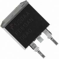
MOSFET N-CH 60V 62A TO-263AB

FDB13AN06A0

Manufacturer Part Number
FDB13AN06A0
Description
MOSFET N-CH 60V 62A TO-263AB
Manufacturer
Fairchild Semiconductor
Series
PowerTrench®r
Type
Power MOSFETr
Datasheet

Specifications of FDB13AN06A0

Fet Type
MOSFET N-Channel, Metal Oxide
Fet Feature
Standard
Rds On (max) @ Id, Vgs
13.5 mOhm @ 62A, 10V
Drain To Source Voltage (vdss)
60V
Current - Continuous Drain (id) @ 25° C
62A
Vgs(th) (max) @ Id
4V @ 250µA
Gate Charge (qg) @ Vgs
29nC @ 10V
Input Capacitance (ciss) @ Vds
1350pF @ 25V
Power - Max
115W
Mounting Type
Surface Mount
Package / Case
D²Pak, TO-263 (2 leads + tab)
Number Of Elements
1
Polarity
N
Channel Mode
Enhancement
Drain-source On-res
0.0135Ohm
Drain-source On-volt
60V
Gate-source Voltage (max)
±20V
Drain Current (max)
10.9A
Power Dissipation
115W
Output Power (max)
Not RequiredW
Frequency (max)
Not RequiredMHz
Noise Figure
Not RequireddB
Power Gain
Not RequireddB
Drain Efficiency
Not Required%
Operating Temp Range
-55C to 175C
Operating Temperature Classification
Military
Mounting
Surface Mount
Pin Count
2 +Tab
Package Type
D2PAK
Configuration
Single
Transistor Polarity
N-Channel
Resistance Drain-source Rds (on)
0.0135 Ohm @ 10 V
Drain-source Breakdown Voltage
60 V
Gate-source Breakdown Voltage
+/- 20 V
Continuous Drain Current
10.9 A
Maximum Operating Temperature
+ 175 C
Mounting Style
SMD/SMT
Minimum Operating Temperature
- 55 C
Lead Free Status / RoHS Status
Lead free / RoHS Compliant
Other names
FDB13AN06A0

Available stocks

Company
Part Number
Manufacturer
Quantity
Price
Part Number:
FDB13AN06A0
Manufacturer:
FAIRCHILD
Quantity:
12 500
Part Number:
FDB13AN06A0
Manufacturer:
FAIRCHILD/仙童
Quantity:
20 000
Company:
Part Number:
FDB13AN06A0
Quantity:
65
©2003 Fairchild Semiconductor Corporation
(FLANGE)
DRAIN
FDB13AN06A0 / FDP13AN06A0
N-Channel PowerTrench
60V, 62A, 13.5m
Features
• r
• Q
• Low Miller Charge
• Low Q
• UIS Capability (Single Pulse and Repetitive Pulse)
• Qualified to AEC Q101
Formerly developmental type 82555
MOSFET Maximum Ratings
Thermal Characteristics
This product has been designed to meet the extreme test conditions and environment demanded by the automotive industry. For a
V
V
I
E
P
T
R
R
R
D
GS
J
DSS
AS
D
Symbol
, T
JC
JA
JA
All Fairchild Semiconductor products are manufactured, assembled and tested under ISO9000 and QS9000 quality systems
DS(ON)
g
(tot) = 22nC (Typ.), V
STG
RR
= 11.5m (Typ.), V
Body Diode
Reliability data can be found at: http://www.fairchildsemi.com/products/discrete/reliability/index.html.
Drain to Source Voltage
Gate to Source Voltage
Drain Current
Continuous (T
Continuous (T
Continuous (T
Pulsed
Single Pulse Avalanche Energy (Note 1)
Power dissipation
Derate above 25
Operating and Storage Temperature
Thermal Resistance Junction to Case TO-220,TO-263
Thermal Resistance Junction to Ambient TO-220,TO-263 (Note 2)
Thermal Resistance Junction to Ambient TO-263, 1in
FDP SERIES
TO-220AB
GS
copy of the requirements, see AEC Q101 at: http://www.aecouncil.com/
A
C
C
GS
= 10V
= 25
= 25
= 100
o
= 10V, I
C
o
o
C, V
C, V
o
C, V
GATE
®
D
DRAIN
GS
GS
= 62A
SOURCE
GS
MOSFET
= 10V, R
= 10V)
Parameter
= 10V)
T
C
= 25°C unless otherwise noted
GATE
JA
SOURCE
certification.
= 43
o
C/W)
FDB SERIES
TO-263AB
Applications
• Motor / Body Load Control
• ABS Systems
• Powertrain Management
• Injection Systems
• DC-DC converters and Off-line UPS
• Distributed Power Architectures and VRMs
• Primary Switch for 12V and 24V systems
2
copper pad area
(FLANGE)
DRAIN
-55 to 175
Ratings
Figure 4
G
10.9
0.77
115
1.3
60
62
44
56
62
43
20
FDB13AN06A0 / FDP13AN06A0 Rev. A1
D
S
July 2003
Units
W/
o
o
o
C/W
C/W
C/W
mJ
o
W
V
V
A
A
A
A
C
o
C

Related parts for FDB13AN06A0

FDB13AN06A0 Summary of contents

Page 1

... GATE SOURCE DRAIN GATE SOURCE TO-263AB FDB SERIES T = 25°C unless otherwise noted C Parameter 10V 10V 10V C/ copper pad area certification. July 2003 D G DRAIN (FLANGE) S Ratings 10.9 Figure 4 56 115 0.77 -55 to 175 1 FDB13AN06A0 / FDP13AN06A0 Rev. A1 Units C/W o C/W o C/W ...

Page 2

... 62A, dI /dt = 100A 62A, dI /dt = 100A Tape Width Quantity 24mm 800 units N/A 50 units Min Typ Max 150 250 100 0.0115 0.0135 - 0.022 0.034 - 0.026 0.030 - 1350 - - 260 - - 2.6 3.4 = 30V DD = 62A - 8 1.0mA - 5 6 158 - 1. 1 FDB13AN06A0 / FDP13AN06A0 Rev. A1 Units ...

Page 3

... Figure 2. Maximum Continuous Drain Current RECTANGULAR PULSE DURATION ( PULSE WIDTH (s) Figure 4. Peak Current Capability 50 75 100 125 150 CASE TEMPERATURE ( C) C Case Temperature NOTES: DUTY FACTOR PEAK FOR TEMPERATURES o ABOVE 25 C DERATE PEAK CURRENT AS FOLLOWS: 175 - 150 - FDB13AN06A0 / FDP13AN06A0 Rev. A1 175 ...

Page 4

... DSS (L/R)ln[(I *R)/(1.3*RATED DSS o STARTING STARTING T = 150 TIME IN AVALANCHE (ms) AV Capability 20V = 10V PULSE DURATION = 80 s DUTY CYCLE = 0.5% MAX 0.5 1.0 1 DRAIN TO SOURCE VOLTAGE ( 10V - 120 160 JUNCTION TEMPERATURE ( C) J FDB13AN06A0 / FDP13AN06A0 Rev +1] DD 100 = 6V 2.0 =62A 200 ...

Page 5

... C) Figure 12. Normalized Drain to Source Breakdown Voltage vs Junction Temperature ISS Figure 14. Gate Charge Waveforms for Constant = 250 A - 120 160 JUNCTION TEMPERATURE ( 30V WAVEFORMS IN DESCENDING ORDER 62A 31A GATE CHARGE (nC) g Gate Current FDB13AN06A0 / FDP13AN06A0 Rev. A1 200 25 ...

Page 6

... Figure 19. Switching Time Test Circuit ©2003 Fairchild Semiconductor Corporation DUT 0.01 Figure 16. Unclamped Energy Waveforms gs2 DUT g(REF) 0 Figure 18. Gate Charge Waveforms d(ON 90 DUT V GS 50% 10% 0 Figure 20. Switching Time Waveforms BV DSS g(TOT g(TH OFF t d(OFF 10% 10% 90% 50% PULSE WIDTH FDB13AN06A0 / FDP13AN06A0 Rev 10V 90% ...

Page 7

... application’s ambient never exceeded (EQ 0.1 is (0.645) DM Figure 21. Thermal Resistance vs Mounting dissipation. Pulse (EQ. 2) Area in Inches Squared (EQ. 3) Area in Centimeters Squared R = 26.51+ 19.84/(0.262+Area) EQ 26.51+ 128/(1.69+Area) EQ (6.45) (64. AREA, TOP COPPER AREA in (cm ) Pad Area FDB13AN06A0 / FDP13AN06A0 Rev ...

Page 8

... PSPICE Electrical Model .SUBCKT FDB13AN06A0 rev August 2002 5.1e- 5.1e-10 Cin 6 8 1.3e-9 Dbody 7 5 DbodyMOD Dbreak 5 11 DbreakMOD Dplcap 10 5 DplcapMOD Ebreak 65.40 Eds Egs Esg Evthres Evtemp GATE Lgate 1 9 6.9e-9 Ldrain 2 5 1.0e-9 Lsource 3 7 2.91e-9 RLgate RLdrain RLsource ...

Page 9

... DPLCAP 10 RSLC2 - 6 ESG 8 EVTHRES + + 19 LGATE EVTEMP 8 RGATE + RLGATE CIN S1A S2A S1B S2B EGS EDS LDRAIN 5 RLDRAIN RSLC1 51 ISCL DBREAK 50 RDRAIN 11 DBODY MWEAK EBREAK MMED + MSTRO 17 18 LSOURCE - 8 7 RSOURCE RLSOURCE RBREAK 17 18 RVTEMP VBAT RVTHRES FDB13AN06A0 / FDP13AN06A0 Rev. A1 DRAIN 2 SOURCE 3 ...

Page 10

... Fairchild Semiconductor Corporation JUNCTION th RTHERM1 CTHERM1 6 RTHERM2 CTHERM2 5 RTHERM3 CTHERM3 4 RTHERM4 CTHERM4 3 RTHERM5 CTHERM5 2 RTHERM6 CTHERM6 tl CASE FDB13AN06A0 / FDP13AN06A0 Rev. A1 ...

Page 11

... TRADEMARKS The following are registered and unregistered trademarks Fairchild Semiconductor owns or is authorized to use and is not intended exhaustive list of all such trademarks. ACEx™ FACT™ ActiveArray™ FACT Quiet Series™ Bottomless™ FAST CoolFET™ FASTr™ CROSSVOLT™ ...

Related keywords