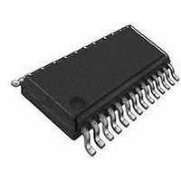
WM8196SCDS Wolfson Microelectronics, WM8196SCDS Datasheet - Page 21

WM8196SCDS
Manufacturer Part Number
WM8196SCDS
Description
Video ICs 16-Bit 12MSPS 3-Channel AFE
Manufacturer
Wolfson Microelectronics
Type
CCD/CISr
Datasheet
1.WM8196SCDS.pdf
(32 pages)
Specifications of WM8196SCDS
Operating Supply Voltage
3.3 V or 5 V
Supply Current
60 mA
Maximum Operating Temperature
+ 70 C
Package / Case
SSOP-28
Conversion Rate
12000 KSPS
Minimum Operating Temperature
- 40 C
Mounting Style
SMD/SMT
Number Of Channels
3
Resolution
16 bit
Lead Free Status / RoHS Status
Lead free / RoHS Compliant
Available stocks
Company
Part Number
Manufacturer
Quantity
Price
Company:
Part Number:
WM8196SCDS
Manufacturer:
Wolfson
Quantity:
6 000
Part Number:
WM8196SCDS
Manufacturer:
WM
Quantity:
20 000
Company:
Part Number:
WM8196SCDS/R
Manufacturer:
PANASONIC
Quantity:
66 562
Part Number:
WM8196SCDS/R
Manufacturer:
WOLFSON
Quantity:
20 000
Part Number:
WM8196SCDS/RV
Manufacturer:
WOLFSON
Quantity:
20 000
WM8196
LINE-BY-LINE OPERATION
w
Certain linear sensors (e.g. Contact Image Sensors) give colour output on a line-by-line basis. i.e. a
full line of red pixels followed by a line of green pixels followed by a line of blue pixels. In order to
accommodate this type of signal the WM8196 can be set into Monochrome mode, with the input
channel switched by writing to control bits CHAN[1:0] between every line. Alternatively, the WM8196
can be placed into colour line-by-line mode by setting the LINEBYLINE control bit. When this bit is
set the green and blue processing channels are powered down and the device is forced internally to
only operate in MONO mode (because only one colour is sampled at a time) through the red channel.
Figure 20 shows the signal path when operating in colour line-by-line mode.
Figure 20 Signal Path When in Line-by-Line Mode
In this mode the input multiplexer and (optionally) the PGA/Offset register multiplexers can be auto-
cycled by the application of pulses to the RLC/ACYC input pin by setting the ACYCNRLC register bit.
See Figure 4 for detailed timing information. The multiplexers change on the first MCLK rising edge
after RLC/ACYC is taken high. A write to the auto-cycle reset register causes these multiplexers to
be reset; selecting the RINP pin and the RED offset/gain registers. Alternatively, all three
multiplexers can be controlled via the serial interface by writing to register bits INTM[1:0] to select the
desired colour. It is also possible for the input multiplexer to be controlled separately from the PGA
and Offset multiplexers. Table 4 describes all the multiplexer selection modes that are possible.
Table 4 Colour Selection Description in Line-by-Line Mode
GINP
RINP
BINP
FME
0
0
1
1
VRLC/VBIAS
ACYCNRLC
RLC
RLC
RLC
DAC
RLC
CL
0
1
0
1
4
INPUT
MUX
Internal,
no force mux
Auto-cycling,
no force mux
Internal,
force mux
Auto-cycling,
force mux
R
CDS
S
V
NAME
S
TIMING CONTROL
VSMP
R
G
B
R
G
B
OFFSET
MUX
MUX
PGA
MCLK
8
Input mux, offset and gain registers determined by
internal register bits INTM1, INTM0.
Input mux, offset and gain registers auto-cycled, RINP
→ GINP → BINP → RINP… on RLC/ACYC pulse.
Input mux selected from internal register bits FM1, FM0;
Offset and gain registers selected from internal register
bits INTM1, INTM0.
Input mux selected from internal register bits FM1, FM0;
Offset and gain registers auto-cycled, RED → GREEN
→ BLUE → RED… on RLC/ACYC pulse.
OFFSET
DAC
+
PGA
8
I/P SIGNAL
POLARITY
ADJUST
DESCRIPTION
+
CONFIGURABLE
PD Rev 4.3 March 2007
ADC
BIT
INTERFACE
16-
PARALLEL
CONTROL
SERIAL/
PORT
DATA
I/O
Production Data
OP[7:0]
SEN/STB
SCK/RNW
SDI/DNA
RLC/ACYC
NRESET
21


