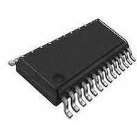
WM8196SCDS Wolfson Microelectronics, WM8196SCDS Datasheet - Page 16

WM8196SCDS
Manufacturer Part Number
WM8196SCDS
Description
Video ICs 16-Bit 12MSPS 3-Channel AFE
Manufacturer
Wolfson Microelectronics
Type
CCD/CISr
Datasheet
1.WM8196SCDS.pdf
(32 pages)
Specifications of WM8196SCDS
Operating Supply Voltage
3.3 V or 5 V
Supply Current
60 mA
Maximum Operating Temperature
+ 70 C
Package / Case
SSOP-28
Conversion Rate
12000 KSPS
Minimum Operating Temperature
- 40 C
Mounting Style
SMD/SMT
Number Of Channels
3
Resolution
16 bit
Lead Free Status / RoHS Status
Lead free / RoHS Compliant
Available stocks
Company
Part Number
Manufacturer
Quantity
Price
Company:
Part Number:
WM8196SCDS
Manufacturer:
Wolfson
Quantity:
6 000
Part Number:
WM8196SCDS
Manufacturer:
WM
Quantity:
20 000
Company:
Part Number:
WM8196SCDS/R
Manufacturer:
PANASONIC
Quantity:
66 562
Part Number:
WM8196SCDS/R
Manufacturer:
WOLFSON
Quantity:
20 000
Part Number:
WM8196SCDS/RV
Manufacturer:
WOLFSON
Quantity:
20 000
WM8196
ADC INPUT BLACK LEVEL ADJUST
OVERALL SIGNAL FLOW SUMMARY
CALCULATING OUTPUT FOR ANY GIVEN INPUT
w
The output from the PGA should be offset to match the full-scale range of the ADC (3V). For
negative-going input video signals, a black level (zero differential) output from the PGA should be
offset to the top of the ADC range by setting register bits PGAFS[1:0]=10. For positive going input
signal the black level should be offset to the bottom of the ADC range by setting PGAFS[1:0]=11.
Bipolar input video is accommodated by setting PGAFS[1:0]=00 or PGAFS[1:0]=01 (zero differential
input voltage gives mid-range ADC output).
Figure 14 represents the processing of the video signal through the WM8196.
Figure 14 Overall Signal Flow
The INPUT SAMPLING BLOCK produces an effective input voltage V
difference between the input video level V
difference between the input video level V
optionally set via the RLC DAC.
The OFFSET DAC BLOCK then adds the amount of fine offset adjustment required to move the
black level of the input signal towards 0V, producing V
The PGA BLOCK then amplifies the white level of the input signal to maximise the ADC range,
outputting voltage V
The ADC BLOCK then converts the analogue signal, V
The digital output is then inverted, if required, through the OUTPUT INVERT BLOCK to produce D
The following equations describe the processing of the video and reset level signals through
the WM8196. The values if V
setup. The PGA value is written first to set the input Voltage range, the Offset DAC is then
adjusted to compensate for any Black/Reset level offsets and finally the RLC DAC value is
set to position the reset level correctly during operation.
Note: Refer to WAN0123 for detailed information on device calibration procedures.
INPUT SAMPLING BLOCK: INPUT SAMPLING AND REFERENCING
If CDS = 1, (i.e. CDS operation) the previously sampled reset level, V
input video.
If CDS = 0, (non-CDS operation) the simultaneously sampled voltage on pin VRLC is subtracted
instead.
If RLCEXT = 1, V
V
V
V
RLCEXT=1
IN
RESET
VRLC
CDS = 0
V
V
CDS = 1
1
1
DAC
RLC
SAMPLING
RLCEXT=0
VRLC
=
=
BLOCK
INPUT
+
See parametrics for
DAC voltages.
3
.
is an externally applied voltage on pin VRLC/VBIAS.
-
V
V
V
1
OFFSET DAC
IN
IN
BLOCK
+ +
- V
- V
1
Offset
DAC
V
RESET
VRLC
2
and V
A = 208/(283-PGA[7:0])
V
260mV*(DAC[7:0]-127.5)/127.5
2
.................................................................... Eqn. 2
................................................................... Eqn. 1
BLOCK
PGA
PGA gain
3
X
IN
are often calculated in reverse order during device
and the input reset level V
V
IN
3
analog
and the voltage on the VRLC/VBIAS pin, V
2
+32768 if PGAFS[1:0]=0x
+0
+65535 if PGAFS[1:0]=10
.
3
, to a 16-bit unsigned digital output, D
x (65535/V
if PGAFS[1:0]=11
ADC BLOCK
FS
V
V
VRLC is voltage applied to VRLC pin
CDS, RLCEXT,RLCV[3:0], DAC[7:0],
PGA[7:0], PGAFS[1:0] and INVOP are set
by programming internal control registers.
CDS=1 for CDS, 0 for non-CDS
)
IN
RESET
is RINP or GINP or BINP
RESET
RESET
is V
D
IN
digital
. For non-CDS this is the
D2 = D1 if INVOP = 0
D2 = 65535-D1 if INVOP = 1
1
1
sampled during reset clamp
. For CDS, this is the
, is subtracted from the
PD Rev 4.3 March 2007
OUTPUT
INVERT
BLOCK
Production Data
D
OP[7:0]
2
1
.
VRLC
2.
16
,


