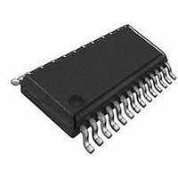
WM8196SCDS Wolfson Microelectronics, WM8196SCDS Datasheet - Page 17

WM8196SCDS
Manufacturer Part Number
WM8196SCDS
Description
Video ICs 16-Bit 12MSPS 3-Channel AFE
Manufacturer
Wolfson Microelectronics
Type
CCD/CISr
Datasheet
1.WM8196SCDS.pdf
(32 pages)
Specifications of WM8196SCDS
Operating Supply Voltage
3.3 V or 5 V
Supply Current
60 mA
Maximum Operating Temperature
+ 70 C
Package / Case
SSOP-28
Conversion Rate
12000 KSPS
Minimum Operating Temperature
- 40 C
Mounting Style
SMD/SMT
Number Of Channels
3
Resolution
16 bit
Lead Free Status / RoHS Status
Lead free / RoHS Compliant
Available stocks
Company
Part Number
Manufacturer
Quantity
Price
Company:
Part Number:
WM8196SCDS
Manufacturer:
Wolfson
Quantity:
6 000
Part Number:
WM8196SCDS
Manufacturer:
WM
Quantity:
20 000
Company:
Part Number:
WM8196SCDS/R
Manufacturer:
PANASONIC
Quantity:
66 562
Part Number:
WM8196SCDS/R
Manufacturer:
WOLFSON
Quantity:
20 000
Part Number:
WM8196SCDS/RV
Manufacturer:
WOLFSON
Quantity:
20 000
WM8196
OUTPUT FORMATS
w
If RLCEXT = 0, V
V
OFFSET DAC BLOCK: OFFSET (BLACK-LEVEL) ADJUST
The resultant signal V
PGA NODE: GAIN ADJUST
The signal is then multiplied by the PGA gain,
ADC BLOCK: ANALOGUE-DIGITAL CONVERSION
The analogue signal is then converted to a 16-bit unsigned number, with input range configured by
PGAFS[1:0].
where the ADC full-scale range, V
OUTPUT INVERT BLOCK: POLARITY ADJUST
The polarity of the digital output may be inverted by control bit INVOP.
The digital data output from the ADC is available to the user in 8 or 4-bit wide multiplexed formats by
setting control bit MUXOP[1:0]. Latency of valid output data with respect to VSMP is programmable
by writing to control bits DEL[1:0]. The latency for each mode is shown in the Operating Mode Timing
Diagrams section.
Figure 15 shows the output data formats for Modes 1 – 2 and 4 – 6. Figure 16 shows the output data
formats for Mode 3. Table 2 summarises the output data obtained for each format.
Figure 15 Output Data Formats
RLCSTEP
4+4+4+4-BIT
OUTPUT
OUTPUT
is the step size of the RLC DAC and V
V
V
V
D
D
D
D
D
8+8-BIT
(Modes 1 − 2, 4 − 6)
MCLK
VRLC
2
3
1
1
1
2
2
[15:0] = INT{ (V
[15:0] = INT{ (V
[15:0] = INT{ (V
[15:0] = D
[15:0] = 65535 – D
VRLC
=
=
=
1
is the output from the internal RLC DAC.
1
A
[15:0]
is added to the Offset DAC output.
A
(V
V
V
B
1
2
3
3
3
RLCSTEP
+ {260mV ∗ (DAC[7:0]-127.5) } / 127.5 ..................... Eqn. 4
∗ 208/(283- PGA[7:0]) .............................................. Eqn. 5
/V
/V
/V
C
1
FS
FS
FS
[15:0]
B
) ∗ 65535} + 32767 PGAFS[1:0] = 00 or 01 ...... Eqn. 6
) ∗ 65535}
) ∗ 65535} + 65535 PGAFS[1:0] = 10 ............... Eqn. 8
FS
D
∗ RLCV[3:0]) + V
= 3V
RLCBOT
Figure 16 Output Data Formats
RLCBOT
PGAFS[1:0] = 11 ............... Eqn. 7
(INVOP = 0) ...................... Eqn. 9
(INVOP = 1) ...................... Eqn. 10
is the minimum output of the RLC DAC.
................................. Eqn. 3
4+4+4+4-BIT
OUTPUT
OUTPUT
(Mode 3)
8+8-BIT
MCLK
A B
PD Rev 4.3 March 2007
A
A B
Production Data
C D
B
17


