FQPF8N80C Fairchild Semiconductor, FQPF8N80C Datasheet
FQPF8N80C
Specifications of FQPF8N80C
Available stocks


Related parts for FQPF8N80C


FQPF8N80C Summary of contents
Page 1
... JC R Thermal Resistance, Case-to-Sink Typ Thermal Resistance, Junction-to-Ambient JA ©2009 Fairchild Semiconductor Corporation FQP8N80C/FQPF8N80C/FQPF8N80CYDTU Rev.A Features • 8A, 800V, R • Low gate charge ( typical 35 nC) • Low Crss ( typical 13 pF) • Fast switching • 100% avalanche tested • Improved dv/dt capability • RoHS Compliant ...
Page 2
... Repetitive Rating : Pulse width limited by maximum junction temperature 25mH 8A 50V Starting ≤ 8A, di/dt ≤ 200A ≤ BV Starting DSS, 4. Pulse Test : Pulse width ≤ 300 s, Duty cycle ≤ Essentially independent of operating temperature FQP8N80C/FQPF8N80C/FQPF8N80CYDTU Rev 25°C unless otherwise noted C Test Conditions 250 250 A, Referenced to 25° 800 ...
Page 3
... Drain Current [A] D Figure 3. On-Resistance Variation vs Drain Current and Gate Voltage 2500 C 2000 iss 1500 C oss 1000 C 500 rss Drain-Source Voltage [V] DS Figure 5. Capacitance Characteristics FQP8N80C/FQPF8N80C/FQPF8N80CYDTU Rev ※ Notes : 1. 250μ s Pulse Test 25℃ Figure 2. Transfer Characteristics ※ Note : T = 25℃ ...
Page 4
... C] Figure 8. On-Resistance Variation 100 Figure 9-2. Maximum Safe Operating Area 100 125 150 4 ※ Notes : 4 - 100 150 200 Junction Temperature [ Temperature Operation in This Area is Limited by R DS(on 100 ※ Notes : 150 Single Pulse Drain-Source Voltage [V] DS for FQPF8N80C www.fairchildsemi.com ...
Page 5
... Typical Characteristics Figure 11-1. Transient Thermal Response Curve for FQP8N80C Figure 11-2. Transient Thermal Response Curve for FQPF8N80C FQP8N80C/FQPF8N80C/FQPF8N80CYDTU Rev.A (Continued) ※ θ tio ※ tio ℃ θ ( ℃ θ ( θ www.fairchildsemi.com ...
Page 6
... FQP8N80C/FQPF8N80C/FQPF8N80CYDTU Rev. A Gate Charge Test Circuit & Waveform Resistive Switching Test Circuit & Waveforms Unclamped Inductive Switching Test Circuit & Waveforms 5 www.fairchildsemi.com ...
Page 7
... FQP8N80C/FQPF8N80C/FQPF8N80CYDTU Rev. A Peak Diode Recovery dv/dt Test Circuit & Waveforms + + • • • I • www.fairchildsemi.com ...
Page 8
... FQP8N80C/FQPF8N80C/FQPF8N80CYDTU Rev. A Peak Diode Recovery dv/dt Test Circuit & Waveforms + + • • • I • www.fairchildsemi.com ...
Page 9
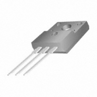
... Package Dimensions 9.90 (8.70) ø3.60 1.27 0.10 2.54TYP [2.54 ] 0.20 10.00 FQP8N80C/FQPF8N80C/FQPF8N80CYDTU Rev.A TO-220 0.20 0.10 1.52 0.10 0.80 0.10 2.54TYP [2.54 ] 0.20 0.20 8 4.50 0.20 +0.10 1.30 –0.05 +0.10 0.50 2.40 0.20 –0.05 Dimensions in Millimeters www.fairchildsemi.com ...
Page 10
... Package Dimensions 10.16 (7.00) MAX1.47 0.80 0.10 #1 0.35 0.10 2.54TYP [2.54 ] 0.20 9.40 FQP8N80C/FQPF8N80C/FQPF8N80CYDTU Rev.A (Continued) TO-220F ø3.18 0.20 0.10 (1.00x45 ) 2.54TYP [2.54 ] 0.20 0.20 9 2.54 0.20 (0.70) +0.10 0.50 2.76 –0.05 0.20 Dimensions in Millimeters www.fairchildsemi.com ...
Page 11
... FQP8N80C/FQPF8N80C/FQPF8N80CYDTU Rev.A 10 www.fairchildsemi.com ...
Page 12
... Definition of Terms Datasheet Identification Product Status Advance Information Formative / In Design Preliminary First Production No Identification Needed Full Production Obsolete Not In Production FQP8N80C/FQPF8N80C/FQPF8N80CYDTU Rev. A ® FRFET Programmable Active Droop™ SM ® Global Power Resource QFET Green FPS™ QS™ Green FPS™ e-Series™ ...