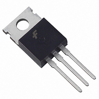
FDP7030BL Fairchild Semiconductor, FDP7030BL Datasheet - Page 4

FDP7030BL
Manufacturer Part Number
FDP7030BL
Description
MOSFET N-CH 30V 60A TO-220
Manufacturer
Fairchild Semiconductor
Series
PowerTrench®r
Datasheet
1.FDB7030BL.pdf
(5 pages)
Specifications of FDP7030BL
Fet Type
MOSFET N-Channel, Metal Oxide
Fet Feature
Logic Level Gate
Rds On (max) @ Id, Vgs
9 mOhm @ 30A, 10V
Drain To Source Voltage (vdss)
30V
Current - Continuous Drain (id) @ 25° C
60A
Vgs(th) (max) @ Id
3V @ 250µA
Gate Charge (qg) @ Vgs
24nC @ 5V
Input Capacitance (ciss) @ Vds
1760pF @ 15V
Power - Max
60W
Mounting Type
Through Hole
Package / Case
TO-220-3 (Straight Leads)
Configuration
Single
Transistor Polarity
N-Channel
Resistance Drain-source Rds (on)
0.009 Ohm @ 10 V
Drain-source Breakdown Voltage
30 V
Gate-source Breakdown Voltage
+/- 20 V
Continuous Drain Current
60 A
Power Dissipation
60000 mW
Maximum Operating Temperature
+ 175 C
Mounting Style
Through Hole
Minimum Operating Temperature
- 65 C
Continuous Drain Current Id
60A
Drain Source Voltage Vds
30V
On Resistance Rds(on)
9mohm
Rds(on) Test Voltage Vgs
10V
Threshold Voltage Vgs Typ
1.9V
Rohs Compliant
Yes
Fall Time
19 ns
Rise Time
12 ns
Lead Free Status / RoHS Status
Lead free / RoHS Compliant
Available stocks
Company
Part Number
Manufacturer
Quantity
Price
Company:
Part Number:
FDP7030BL
Manufacturer:
FAIRCHILD
Quantity:
161
Company:
Part Number:
FDP7030BL
Manufacturer:
FAIRCHILD
Quantity:
12 500
Part Number:
FDP7030BL
Manufacturer:
ON/安森美
Quantity:
20 000
Typical Characteristics
1000
10
100
8
6
4
2
0
Figure 9. Maximum Safe Operating Area.
10
0
1
Figure 7. Gate Charge Characteristics.
0.1
I
D
0.01
0.1
= 30A
0.00001
1
SINGLE PULSE
R
R
DS(ON)
V
JC
T
5
GS
A
= 2.5
= 25
= 10V
LIMIT
o
o
D = 0.5
C/W
C
V
10
DS
0.2
0.1
, DRAIN-SOURCE VOLTAGE (V)
0.05
Q
0.02
g
1
, GATE CHARGE (nC)
0.01
SINGLE PULSE
15
0.0001
DC
Figure 11. Transient Thermal Response Curve.
20
100m
V
10mS
DS
= 10V
1mS
10
25
100µs
15V
10µs
30
20V
0.001
100
35
t
1
, TIME (sec)
2500
2000
1500
1000
5000
4000
3000
2000
1000
500
0.00001
0
0
0
Figure 8. Capacitance Characteristics.
Figure 10. Single Pulse Maximum
C
rss
0.01
5
0.0001
V
Power Dissipation.
C
DS
oss
, DRAIN TO SOURCE VOLTAGE (V)
10
0.001
t
1
, TIME (sec)
15
0.1
0.01
FDP7030BL/FDB7030BL Rev D1(W)
Duty Cycle, D = t
T
R
P(pk
J
R
20
JC
- T
JC
(t) = r(t) * R
C
A
= 2.5 °C/W
iss
t
= P * R
SINGLE PULSE
R
1
t
2
0.1
JC
T
A
= 2.5°C/W
25
= 25°C
V
f = 1MHz
JC
1
GS
JC
(t)
/ t
= 0 V
2
1
30
1


