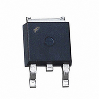
FDD3670 Fairchild Semiconductor, FDD3670 Datasheet - Page 4

FDD3670
Manufacturer Part Number
FDD3670
Description
MOSFET N-CH 100V 34A D-PAK
Manufacturer
Fairchild Semiconductor
Series
PowerTrench®r
Datasheet
1.FDD3670.pdf
(5 pages)
Specifications of FDD3670
Fet Type
MOSFET N-Channel, Metal Oxide
Fet Feature
Logic Level Gate
Rds On (max) @ Id, Vgs
32 mOhm @ 7.3A, 10V
Drain To Source Voltage (vdss)
100V
Current - Continuous Drain (id) @ 25° C
34A
Vgs(th) (max) @ Id
4V @ 250µA
Gate Charge (qg) @ Vgs
80nC @ 10V
Input Capacitance (ciss) @ Vds
2490pF @ 50V
Power - Max
1.6W
Mounting Type
Surface Mount
Package / Case
DPak, TO-252 (2 leads+tab), SC-63
Lead Free Status / RoHS Status
Lead free / RoHS Compliant
Available stocks
Company
Part Number
Manufacturer
Quantity
Price
Company:
Part Number:
FDD3670
Manufacturer:
FAIRCHILD
Quantity:
30 000
Typical Characteristics
10
1000
0.01
8
6
4
2
0
100
0.1
Figure 9. Maximum Safe Operating Area.
10
0
1
Figure 7. Gate Charge Characteristics.
0.1
I
0.0001
D
0.001
= 7.3A
0.01
SINGLE PULSE
R
0.1
R
V
0.0001
JA
T
DS(ON)
1
GS
A
10
= 96
= 25
= 10V
LIMIT
o
D = 0.5
o
C/W
C
V
0.2
1
0.1
DS
0.05
, DRAIN-SOURCE VOLTAGE (V)
0.02
20
Q
0.01
g
, GATE CHARGE (nC)
SINGLE PULSE
DC
10s
0.001
1s
100ms
30
10
10ms
Figure 11. Transient Thermal Response Curve.
Thermal characterization performed using the conditions described in Note 1b.
Transient thermal response will change depending on the circuit board design.
1ms
V
100 s
DS
40
= 20V
100
0.01
80V
50
50V
1000
60
0.1
4500
4000
3500
3000
2500
2000
1500
1000
40
30
20
10
500
0
0.1
0
Figure 8. Capacitance Characteristics.
0
Figure 10. Single Pulse Maximum
1
20
V
1
Power Dissipation.
DS
, DRAIN TO SOURCE VOLTAGE (V)
t
40
1
, TIME (sec)
10
10
C
C
OSS
ISS
60
P(pk)
Duty Cycle, D = t
C
T
R
RSS
J
R
JA
100
- T
SINGLE PULSE
100
R
JA
(t) = r(t) + R
A
T
JA
t
1
= 96 °C/W
A
80
= P * R
t
= 96°C/W
= 25°C
2
FDD3670 Rev C(W)
V
f = 1MHz
GS
= 0 V
JA
1
(t)
JA
/ t
1000
100
2
1000


