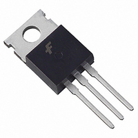
FQP9P25 Fairchild Semiconductor, FQP9P25 Datasheet - Page 3

FQP9P25
Manufacturer Part Number
FQP9P25
Description
MOSFET P-CH 250V 9.4A TO-220
Manufacturer
Fairchild Semiconductor
Series
QFET™r
Datasheet
1.FQP9P25.pdf
(8 pages)
Specifications of FQP9P25
Fet Type
MOSFET P-Channel, Metal Oxide
Fet Feature
Standard
Rds On (max) @ Id, Vgs
620 mOhm @ 4.7A, 10V
Drain To Source Voltage (vdss)
250V
Current - Continuous Drain (id) @ 25° C
9.4A
Vgs(th) (max) @ Id
5V @ 250µA
Gate Charge (qg) @ Vgs
38nC @ 10V
Input Capacitance (ciss) @ Vds
1180pF @ 25V
Power - Max
120W
Mounting Type
Through Hole
Package / Case
TO-220-3 (Straight Leads)
Configuration
Single
Transistor Polarity
P-Channel
Resistance Drain-source Rds (on)
0.62 Ohm @ 10 V
Forward Transconductance Gfs (max / Min)
5.7 S
Drain-source Breakdown Voltage
250 V
Gate-source Breakdown Voltage
+/- 30 V
Continuous Drain Current
9.4 A
Power Dissipation
120000 mW
Maximum Operating Temperature
+ 150 C
Mounting Style
Through Hole
Minimum Operating Temperature
- 55 C
Lead Free Status / RoHS Status
Lead free / RoHS Compliant
Available stocks
Company
Part Number
Manufacturer
Quantity
Price
Company:
Part Number:
FQP9P25
Manufacturer:
FSC
Quantity:
45 000
Company:
Part Number:
FQP9P25
Manufacturer:
INFINEON
Quantity:
3 000
Part Number:
FQP9P25
Manufacturer:
FAIRCHILD/仙童
Quantity:
20 000
©2000 Fairchild Semiconductor International
Typical Characteristics
2400
2000
1600
1200
800
400
10
2.0
1.5
1.0
0.5
0.0
10
10
-1
0
1
0
10
10
0
Figure 5. Capacitance Characteristics
-1
-1
Figure 3. On-Resistance Variation vs.
Top :
Bottom : -5.5 V
Figure 1. On-Region Characteristics
Drain Current and Gate Voltage
-15.0 V
-10.0 V
-8.0 V
-7.0 V
-6.5 V
-6.0 V
V
GS
10
-V
-V
DS
DS
, Drain-Source Voltage [V]
, Drain-Source Voltage [V]
-I
D
10
10
, Drain Current [A]
0
0
V
GS
= - 20V
V
C
GS
C
C
20
oss
iss
rss
= - 10V
C
C
C
iss
oss
rss
※ Notes :
= C
= C
= C
10
10
※ Note : T
1. 250μ s Pulse Test
2. T
30
gs
ds
gd
1
1
C
+ C
+ C
= 25℃
gd
※ Notes :
gd
(C
1. V
2. f = 1 MHz
J
ds
= 25℃
GS
= shorted)
= 0 V
40
10
10
10
10
10
10
12
10
8
6
4
2
0
-1
-1
1
0
1
0
0.0
0
2
Figure 4. Body Diode Forward Voltage
Figure 6. Gate Charge Characteristics
Figure 2. Transfer Characteristics
5
Variation vs. Source Current
0.5
25℃
150℃
150℃
4
-V
-V
10
Q
SD
and Temperature
GS
G
1.0
25℃
, Source-Drain Voltage [V]
, Total Gate Charge [nC]
, Gate-Source Voltage [V]
V
DS
V
DS
= -200V
15
V
DS
= -125V
-55℃
= -50V
1.5
6
20
2.0
※ Notes :
25
※ Notes :
1. V
2. 250μ s Pulse Test
1. V
2. 250μ s Pulse Test
※ Note : I
8
DS
GS
= -50V
= 0V
2.5
30
D
= -9.4 A
Rev. A2, December 2000
3.0
10
35


