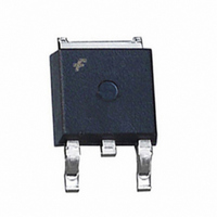
FDD306P Fairchild Semiconductor, FDD306P Datasheet - Page 3

FDD306P
Manufacturer Part Number
FDD306P
Description
MOSFET P-CH 12V 6.7A D-PAK
Manufacturer
Fairchild Semiconductor
Series
PowerTrench®r
Datasheet
1.FDD306P.pdf
(5 pages)
Specifications of FDD306P
Fet Type
MOSFET P-Channel, Metal Oxide
Fet Feature
Logic Level Gate
Rds On (max) @ Id, Vgs
28 mOhm @ 6.7A, 4.5V
Drain To Source Voltage (vdss)
12V
Current - Continuous Drain (id) @ 25° C
6.7A
Vgs(th) (max) @ Id
1.5V @ 250µA
Gate Charge (qg) @ Vgs
21nC @ 4.5V
Input Capacitance (ciss) @ Vds
1290pF @ 6V
Power - Max
1.6W
Mounting Type
Surface Mount
Package / Case
DPak, TO-252 (2 leads+tab), SC-63
Transistor Polarity
P Channel
Continuous Drain Current Id
6.7A
Drain Source Voltage Vds
12V
On Resistance Rds(on)
90mohm
Rds(on) Test Voltage Vgs
-4.5V
Threshold Voltage Vgs Typ
-500mV
Rohs Compliant
Yes
Configuration
Single
Resistance Drain-source Rds (on)
0.028 Ohms
Drain-source Breakdown Voltage
- 12 V
Gate-source Breakdown Voltage
+/- 8 V
Continuous Drain Current
6.7 A
Power Dissipation
52 W
Maximum Operating Temperature
+ 175 C
Mounting Style
SMD/SMT
Minimum Operating Temperature
- 55 C
Lead Free Status / RoHS Status
Lead free / RoHS Compliant
Available stocks
Company
Part Number
Manufacturer
Quantity
Price
Part Number:
FDD306P
Manufacturer:
FAIRCHILD/仙童
Quantity:
20 000
FDD306P Rev. C
Typical Characteristics
1.4
1.3
1.2
1.1
0.9
0.8
54
45
36
27
18
54
45
36
27
18
9
0
1
9
0
-50
0
0
V
I
GS
D
V
V
Figure 1. On-Region Characteristics.
Figure 3. On-Resistance Variation
= -6.7A
DS
GS
= -4.5V
-25
Figure 5. Transfer Characteristics.
= - 5V
= -4.5V
-4.0V
0
T
-V
J
1
1
, JUNCTION TEMPERATURE (°C)
GS
-V
withTemperature.
, GATE TO SOURCE VOLTAGE (V)
DS
25
, DRAIN-SOURCE VOLTAGE (V)
50
-3.5V
2
2
75
T
A
= -55°C
-3.0V
100
-2.5V
125
3
3
-2.0V
25°C
150
125°C
-1.8V
175
4
4
3
0.0001
0.001
Figure 6. Body Diode Forward Voltage Variation
0.08
0.06
0.04
0.02
0.01
100
2.5
1.5
0.5
0.1
0.1
10
2
1
0
1
0
0
0
Figure 2. On-Resistance Variation with
Figure 4. On-Resistance Variation with
with Source Current and Temperature.
V
V
T
GS
GS
A
= 25°C
= 0V
= -1.8V
Drain Current and Gate Voltage.
T
0.2
-V
9
A
= 125°C
SD
2
Gate-to-Source Voltage.
, BODY DIODE FORWARD VOLTAGE (V)
-2.0V
-V
GS
, GATE TO SOURCE VOLTAGE (V)
0.4
18
-I
D
, DRAIN CURRENT (A)
T
25°C
A
-2.5V
= 125°C
4
0.6
27
-55°C
-3.0V
6
0.8
36
-3.5V
45
www.fairchildsemi.com
8
1
I
D
-4.5V
= -3.4A
1.2
54
10


